


- Effect of Na₂SO₃ inhibitor on the structural and morphological properties of PbSe thin films prepared by chemical bath deposition
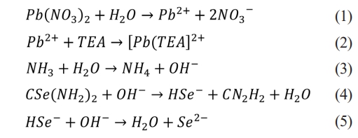
Metehan Önal*
Bilecik Seyh Edebali University, Bilecik, 11210, Turkey
This article is an open access article distributed under the terms of the Creative Commons Attribution Non-Commercial License (http://creativecommons.org/licenses/by-nc/4.0) which permits unrestricted non-commercial use, distribution, and reproduction in any medium, provided the original work is properly cited.
This study investigates the effects of using inhibitors during the deposition of PbSe films by Chemical Bath Deposition method. No prior research has addressed the role of inhibitors in the chemical bath deposition of PbSe films. In this study, the effect of the inhibitor on PbSe films was investigated for the first time. Structural characterization was performed using the data derived from XRD analysis. Analyses showed that inhibitor addition significantly reduced the sizes of crystallites in deposited films, with sizes varying between 45.44 nm and 33.94 nm. The four-probe method was employed to measure the surface resistivity of the films, and it was observed that the resistance increased by up to 30-fold depending on the presence of the inhibitor. SEM and EDX measurements were employed to investigate the surface morphology and chemical composition of the films, respectively. While the use of inhibitors was found to influence the grain structure, EDX analysis indicated that the films were selenium-rich in terms of atomic percentage. Images of the films demonstrated that PbSe adhered uniformly and compactly to the surfaces of the glass substrates.
Keywords: PbSe, CBD, Inhibitor, Semiconductor films.
Nanocrystalline semiconductors have attracted considerable attention for technological applications owing to their remarkable chemical and physical properties [1]. Although significant progress has been achieved in thin-film synthesis, the development of cost-effective, scalable, and high-efficiency deposition techniques continues to represent a major challenge in materials science [2]. Various metal-chalcogenide semiconductors, including cadmium sulfide (CdS), lead sulfide (PbS), cadmium telluride (CdTe), cadmium selenide (CdSe), indium arsenide (InAs), antimony trisulfide (Sb₂S₃), and lead selenide (PbSe), have been extensively employed in the synthesis of thin films for solar cell applications [3]. Consequently, metal-chalcogenide semiconductors have numerous applications in electronics, optoelectronics, and thermoelectrics, including infrared (IR) light emitters and lasers, as well as mid-IR detectors [4-6]. By focusing more on semiconductor materials, researchers are striving to further exploit the properties of metal chalcogenide materials and expand their practical applications [7].
Several fabrication methods are used for the production of lead selenide thin films, including electrodeposition, chemical bath deposition (CBD), electrochemical atomic layer deposition, thermal evaporation, radio frequency (RF) magnetron sputtering, photochemical approaches, molecular beam epitaxy, and pulsed laser deposition [8, 9]. These methods used to produce PbSe offer various advantages, including cost, applicability to large surfaces, crystallinity, and improved film quality, enabling its use in electronic and optoelectronic applications [9-11]. Among existing deposition techniques, CBD is preferred due to its advantages, such as the ability to produce homogeneous films at low temperatures, at low costs, and in a scalable manner, and the ability to improve the crystallographic quality of the films [12-14].
PbSe has a direct optical band gap of approximately 0.27 eV at room temperature. Because it exhibits strong quantum size effects, the energy band gap of its nanocrystals can be tuned to different values between 0.27 eV and 4.5 eV [15]. Lead chalcogenides crystallize in a face-centered cubic (fcc) structure with the space group Fm3m, which is analogous to the crystal structure of sodium chloride (NaCl) [16].
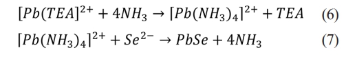
The mechanism underlying the formation of PbSe thin films can be described by the following chemical equations.
The literature review showed that numerous variables affecting the fabrication of PbSe films have been systematically investigated. Some of the research themes are summarized below. Using sodium hydroxide (NaOH) as a complexing agent, the effects of concentration on the thickness, energy band gap, optical properties, and microstructure of PbSe films were analyzed [17]. The effect of extended holding time on the crystal structure and optical properties of PbSe films was investigated by selecting deposition times of 30, 60, 90, and 120 min on Si(100) substrates at a deposition solution temperature of 70 °C [7]. The effects of increasing the bath temperature from 20 °C to 85 °C on the efficiency of PbSe films were investigated [8]. The composition, structure, and functional properties of annealed PbSe films chemically deposited in the presence of various antioxidants and ammonium iodide were investigated [11]. The structural and optical properties of PbSe thin films produced in a chemical bath with pH values ranging from 5 to 8 were analyzed [18]. PbSe films were deposited at constant bath temperature and deposition periods ranging from 3 to 5 hours, and the effect of deposition periods on the structural and thermoelectric properties was investigated [12].
No studies have been identified in the literature that specifically address the reaction rate on PbSe films. However, studies investigating the effects of reaction rate on PbS, ZnS, and CdS thin films produced using the CBD method have appeared in the literature [19-22].
The impact of reaction rate on PbSe films produced using CBD was investigated in my study. Na₂SO₃ was utilized as an inhibitor to reduce the reaction rate. This is the inaugural study in the literature regarding the synthesis of PbSe films with Na₂SO₃ as an inhibitor. The use of an inhibitor slowed down the deposition of PbSe films, leading to a reduction in crystallite size from 44 nm to approximately 34 nm. Additionally, the average surface roughness of the films decreased from 27 nm to 17 nm, while the surface resistance increased from 0.207 kΩ cm to 6.585 kΩ cm. It was also observed that the addition of an inhibitor changed the surface morphology of the films. These results indicate that inhibitors can play critical roles in controlling film growth mechanisms and optimizing material properties for optoelectronic technologies.
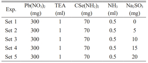
PbSe films were synthesized using CBD. Glass substrates were cleaned with alcohol, rinsed with deionized water, and immersed in 100 mL of deionized water in the bath vessel. The precursor solution was prepared by dissolving 300 mg of Pb(NO₃)₂, followed by the sequential addition of 1 mL triethanolamine (TEA), 0.5 mL ammonia (NH₃), and 70 mg selenourea (CSe(NH₂)₂). The first film was synthesized without an inhibitor, whereas subsequent films were produced by adding Na₂SO₃ in amounts of 5, 10, 15, and 20 mg. The produced films were named as Set 0, Set 1, Set 2, Set 3, and Set 4 according to the concentration of Na₂SO₃ added to the solution. For all films, the deposition periods were 60 minutes, the solution temperature was 23 °C, and the pH was 10.5. A summary of the reaction parameters is provided in Table 1.
In the reference experiment (Set 0), the addition of selenourea caused the solution to turn black within 5 seconds, indicating that the reaction and hence the coating process had begun. In contrast, when an inhibitor was introduced, the blackening of the solution was delayed, occurring within 5-15 minutes, depending on the inhibitor concentration.
Na₂SO₃ acts as a reducing and complexing agent in the bath. Sulfide ions can interact with intermediate selenium species, partially suppressing the rapid decomposition of selenourea and slowing the availability of free Se²⁻ ions in solution. This delayed ion release reduces homogeneous nucleation in the bulk solution, consequently delaying the bath's noticeable darkening [23].
Structural characterization was carried out using X-ray diffraction (XRD) with a BRUKER AXS D8 ADVANCE diffractometer. Film thickness and surface morphology were determined from SEM images, and elemental composition was analyzed with a Zeiss SUPRA 40VP SEM equipped with EDS. The roughness of film surfaces was evaluated from SEM images using ImageJ software, while the surface resistivity of the thin films was determined by the four-probe method.
Structural analysis of PbSe films
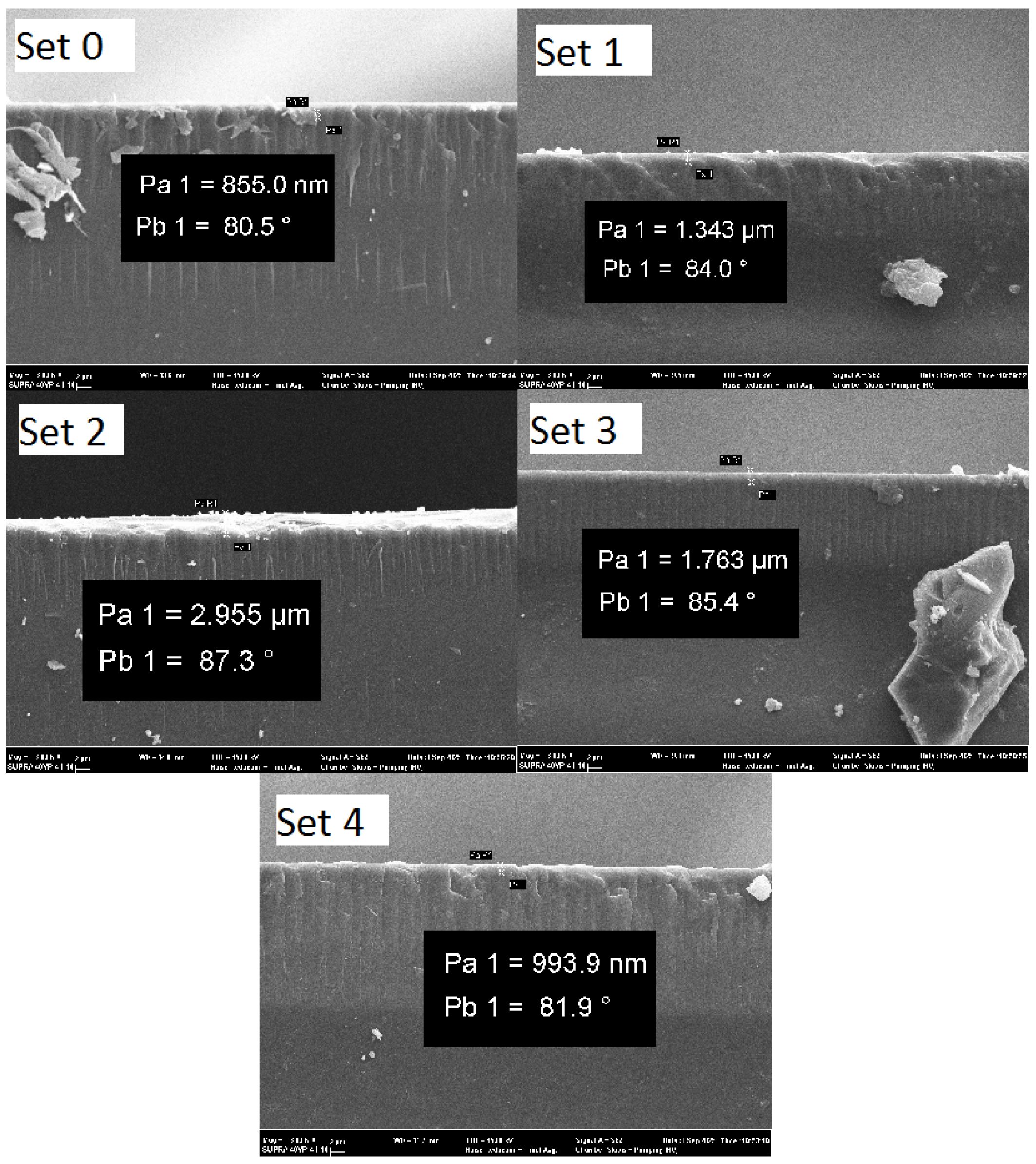
Film thicknesses obtained from SEM images are presented in Fig. 1, with the minimum thickness of 855 nm observed in the reference experiment and the maximum thickness of 2955 nm observed in Set 3. At the end of the experiment, a substantial amount of chemical residue was observed in the reference bath. The residue decreased noticeably in the bath containing 10 mg of inhibitor; however, further increasing the inhibitor concentration resulted in an increase in residue formation. This phenomenon is attributed to heterogeneous nucleation occurring when 10 mg of Na₂SO₃ is used, which is consistent with literature reports emphasizing the role of surface energy manipulation in improving crystallization outcomes [24].
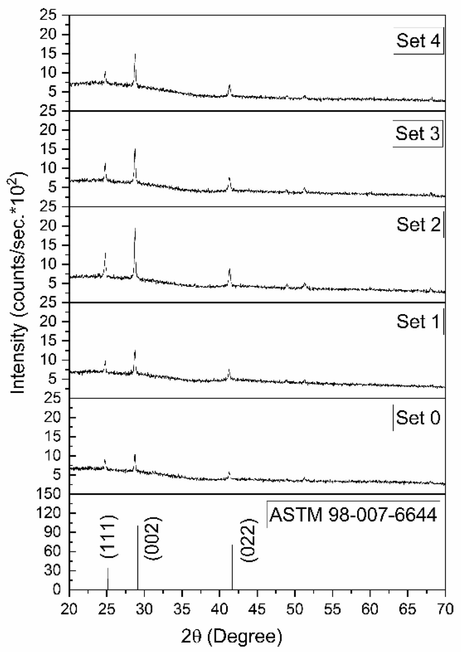
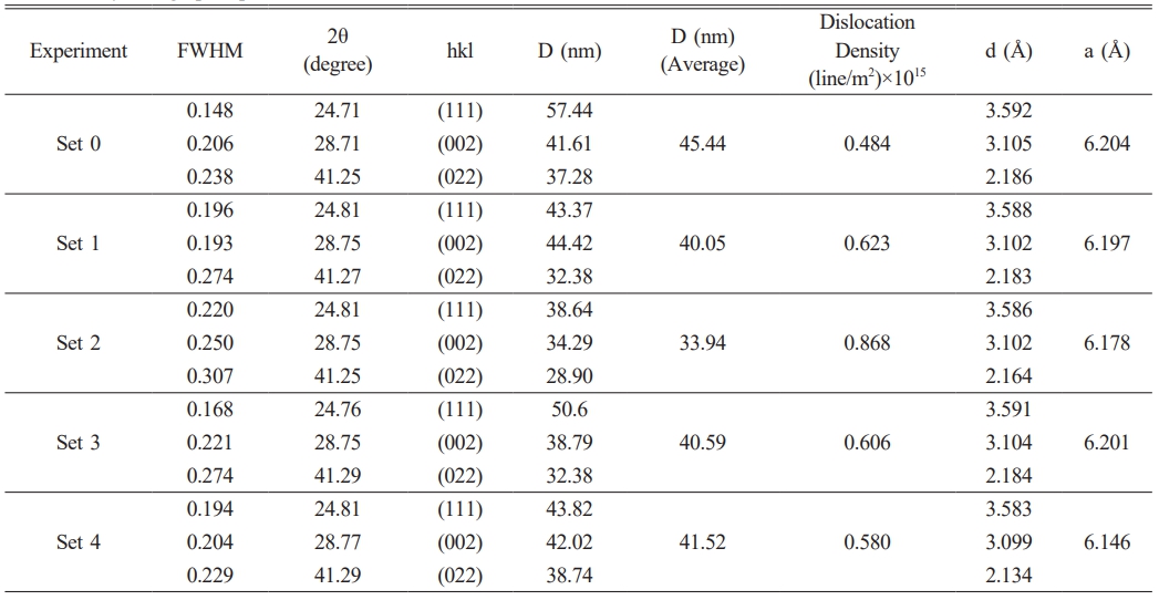
Fig. 2 presents the XRD patterns, showing that all films crystallized in a cubic phase consistent with the ASTM reference card No. 98-007-6644. Examination of Fig. 2 reveals a correlation between film thickness and peak intensity, as expected. The crystallographic parameters derived from the XRD data are presented in Table 2. Table 2 also presents the FWHM values obtained with Origin software and the crystallite sizes estimated using the Debye–Scherrer equation, provided in Eq. (8) [25-27].

Here, D denotes the crystallite size, k is Scherrer’s constant, λ is the X-ray wavelength (1.5405 Å for the present CuKα radiation), β represents the full width at half maximum (FWHM), and θ is the Bragg diffraction angle. The crystallite size obtained in Set 2 was found to be 25% smaller than that in the reference experiment (Set 0). A low crystallite size is particularly desirable for certain applications. This is because crystallite size directly determines electrical, optical, and surface properties. As crystallite size decreases, the surface-to-volume ratio increases. P-type films with a high surface area become more sensitive in gas sensors. Furthermore, as the crystallite size decreases, the band gap increases. Therefore, PbSe can be used not only in the mid-IR but also in near-IR detectors, optoelectronic devices, and photovoltaics.
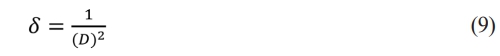
Dislocation density (d ) was calculated using Equation (9) [28, 29], and the value obtained in Set 2 was 1.8 times higher than that of Set 0.
Eq. (10) was employed to determine the lattice parameters of the cubic phase. This equation is given below:

Here, (hkl) are the Miller indices, d is the interplanar spacing, and a is the lattice parameter [30]. As given in Table 2, the parameter values of the lattice of the films were calculated to be between 6.146 and 6.204. Since these values exceed the standard value of 6.122 provided by the ASTM card, it can be inferred that the films are under stress.
Surface properties of the PbSe films
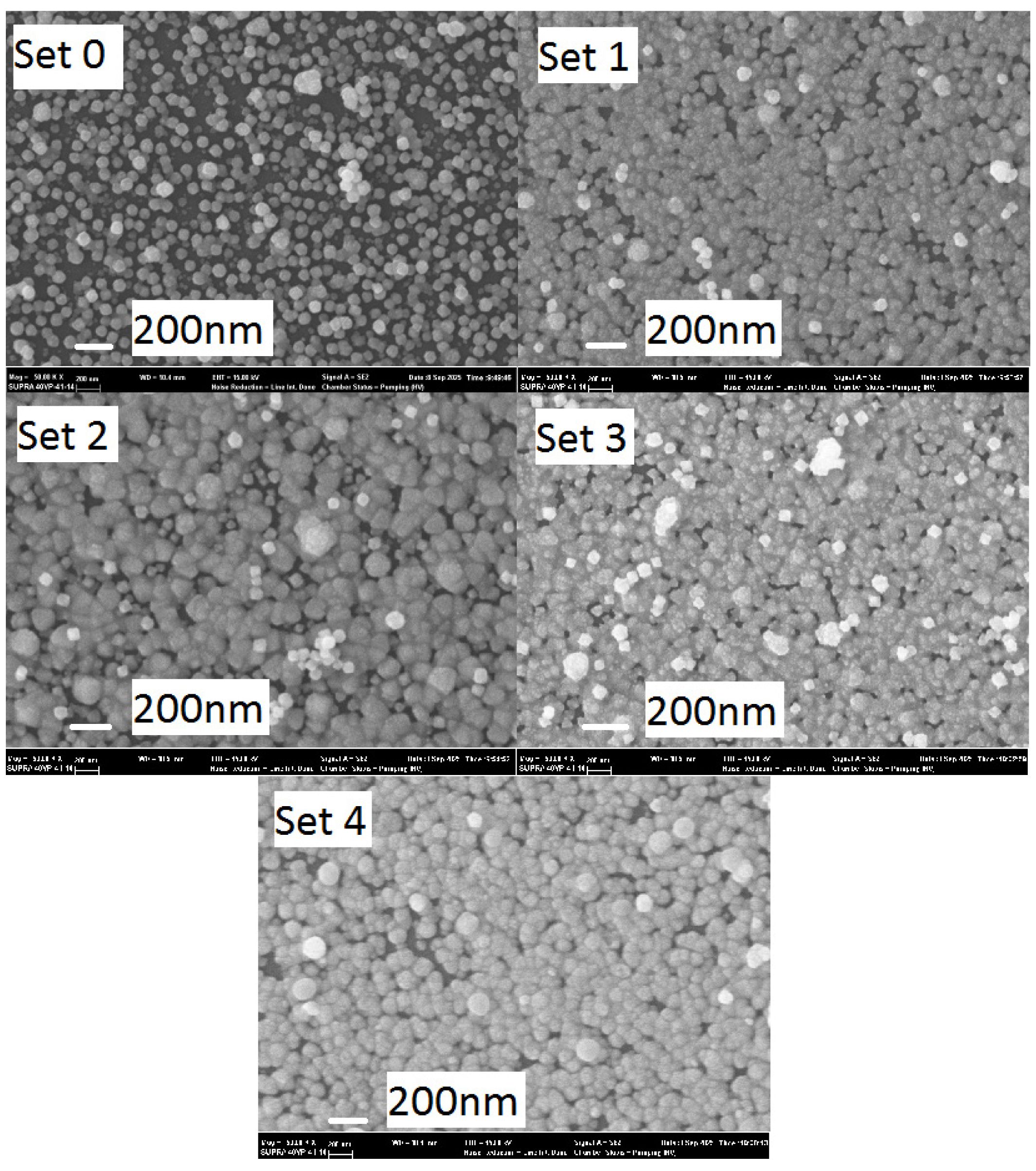
A magnification of 50 kX was used to analyze the SEM images of the PbSe films, as shown in Fig. 3. The images revealed that all glass substrate surfaces were homogeneously coated and free of structural defects such as cracks or pinholes. The average grain size of the film obtained from Set0 was determined to be approximately 100 nm. The grain sizes observed in the films obtained with inhibitors were larger. However, these structures exhibited a cauliflower-like morphology and were composed of smaller grains. This finding is supported by the consistency of the crystallite size values obtained from the XRD results. SEM images of PbSe films with a cauliflower structure obtained with CBD have not been found in the literature. Therefore, this study can be said to be the first time that films with this structure have been produced.
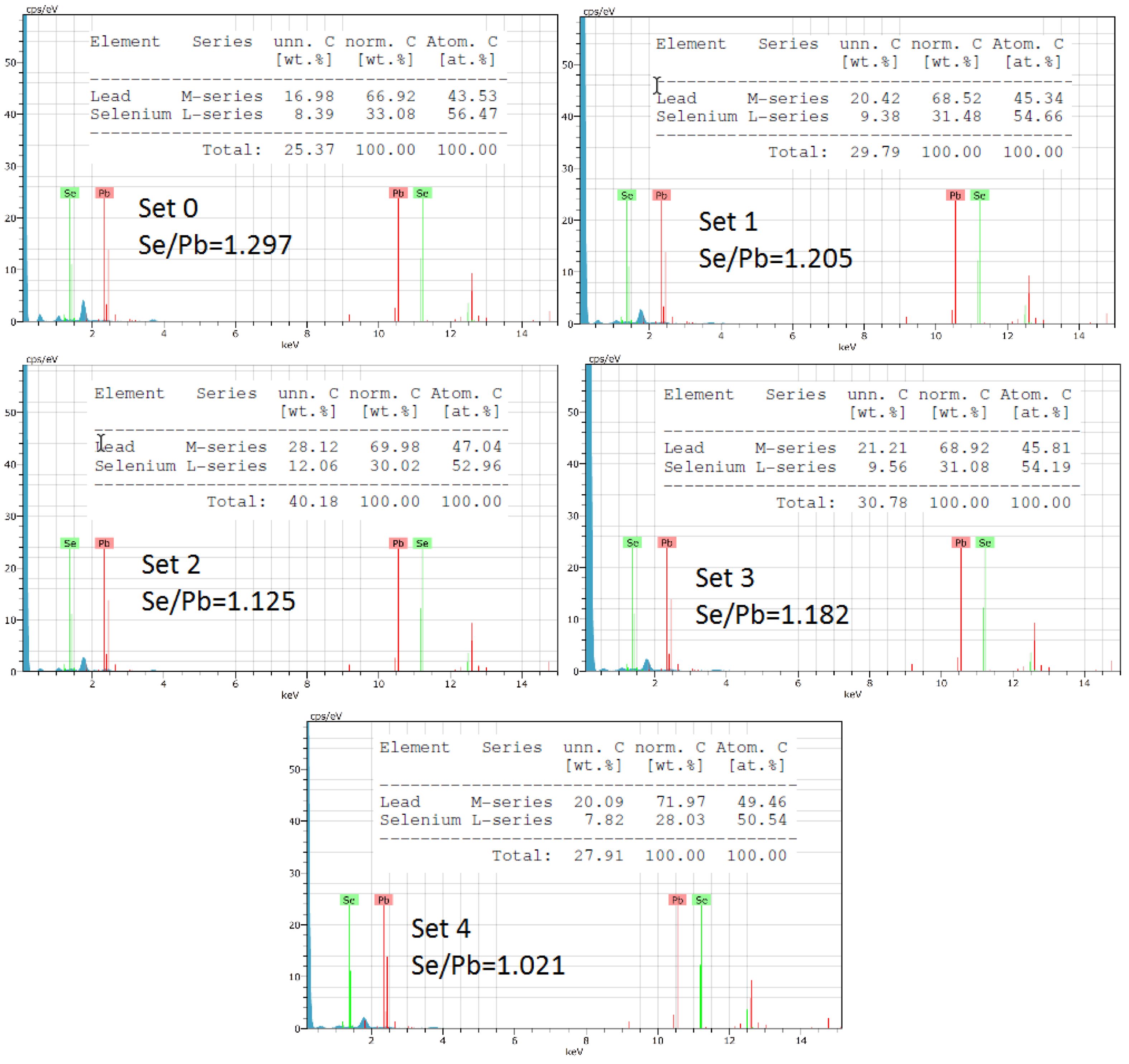
Elemental analysis of the films was performed using EDX to determine the conductivity type of the films. It is known that the type of conductivity of PbSe films depends on their elemental content. Films with a high Pb content are n-type, while films with a high Se content are p-type [31]. This analysis showed that the produced films were Se-rich and concluded that the films had p-type conductivity. Furthermore, as the amount of inhibitor used increased, the Se/Pb ratio almost approached 1. Graphs showing the Se/Pb ratio are given in Fig. 4.
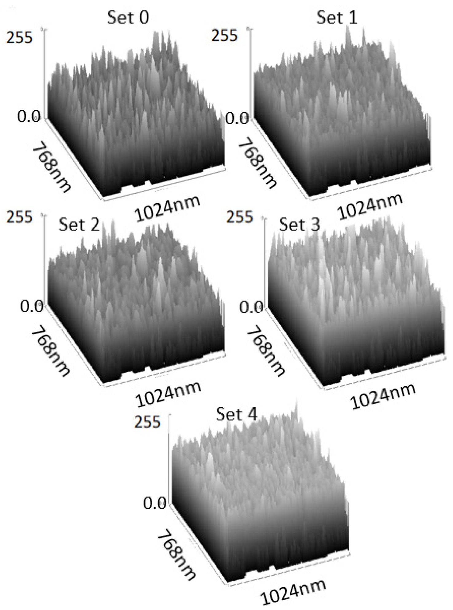
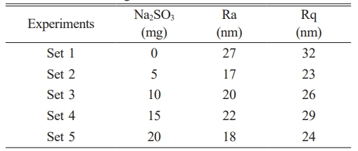
ImageJ software was used to process SEM pictures in order to examine the materials’ surface roughness. ImageJ software was used in numerous research in the literature to analyze surface morphology [32-34]. The average and rms surface roughness values of the films were calculated and are given in Table 3. Surface roughness graphs were also obtained, and these graphs are presented in Fig. 5. Ra values vary between 17 nm and 27 nm, and Rq values vary between 23 nm and 32 nm. There is only one study producing PbSe under the same conditions [35]. In that study, surface roughness values for Ra and Rq were given as 18-26 nm and 22-29.9 nm, respectively. The very similar results obtained in both studies indicate that the use of inhibitors did not alter the roughness of the films.
Sheet resistivity characteristics of PbSe films
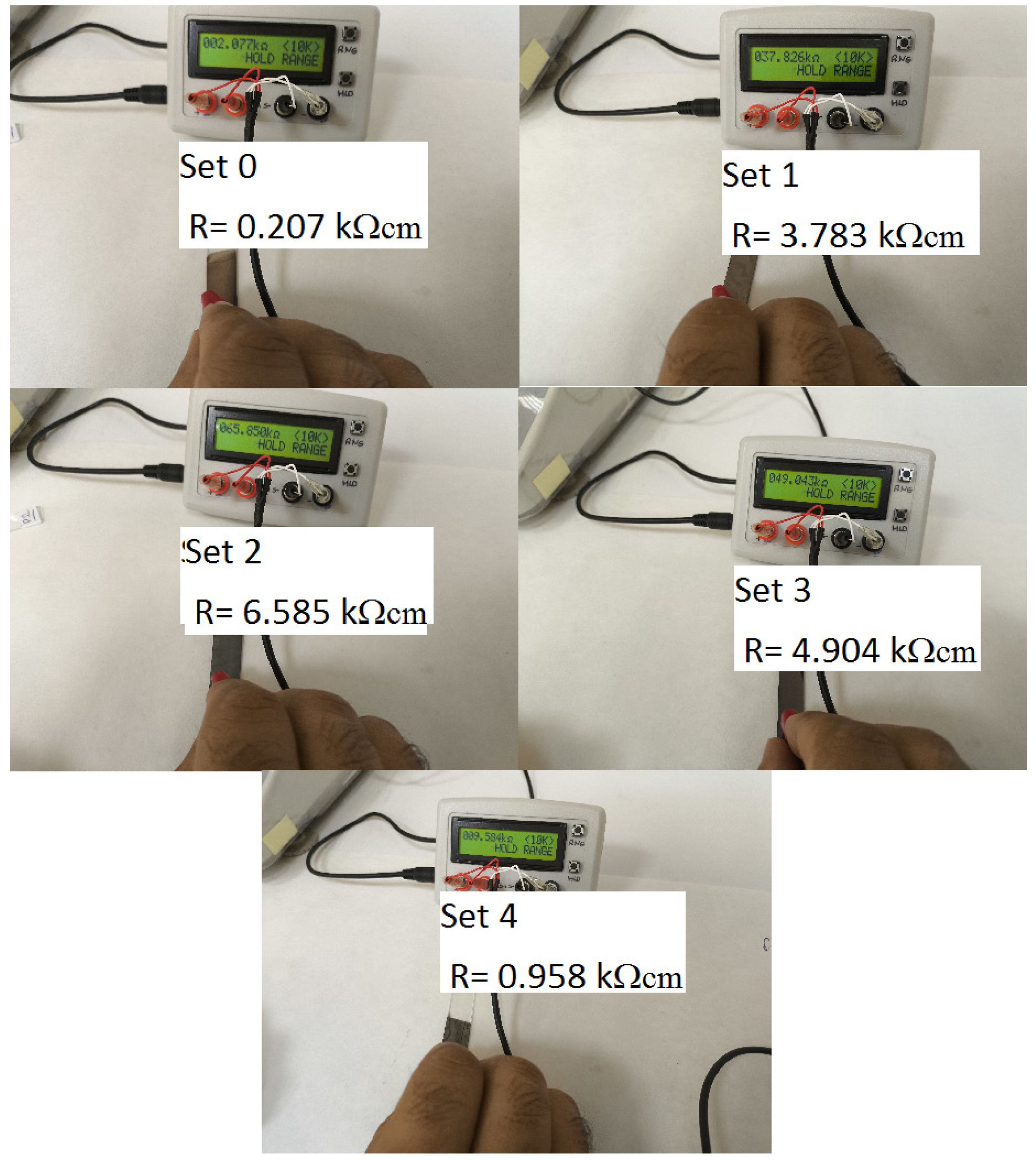
The four-probe method was used to determine the surface resistivity values of PbSe films, and the measurement results are shown in Fig. 6. Analysis of the measurement results revealed that surface resistivity values increased by up to 30-fold due to inhibitor use. Thicker films generally provide more continuous transmission paths, which can reduce resistance; however, in this study, the observed increase in resistance despite thickness suggests that microstructural factors play a dominant role. Specifically, point defects or structural abnormalities, which can act as trap states, can have an effect that further increases resistance. This increase is believed to be due to the reduction in crystallite size due to inhibitor use. It is concluded that decreasing crystallite size increases grain boundaries, which in turn causes electron scattering, leading to increased surface resistivity values. Lower conductivity (high resistivity) results in less leakage current and thus better detector sensitivity. It also reduces dark current, resulting in lower noise and higher sensitivity.
Visual analysis of the PbSe films
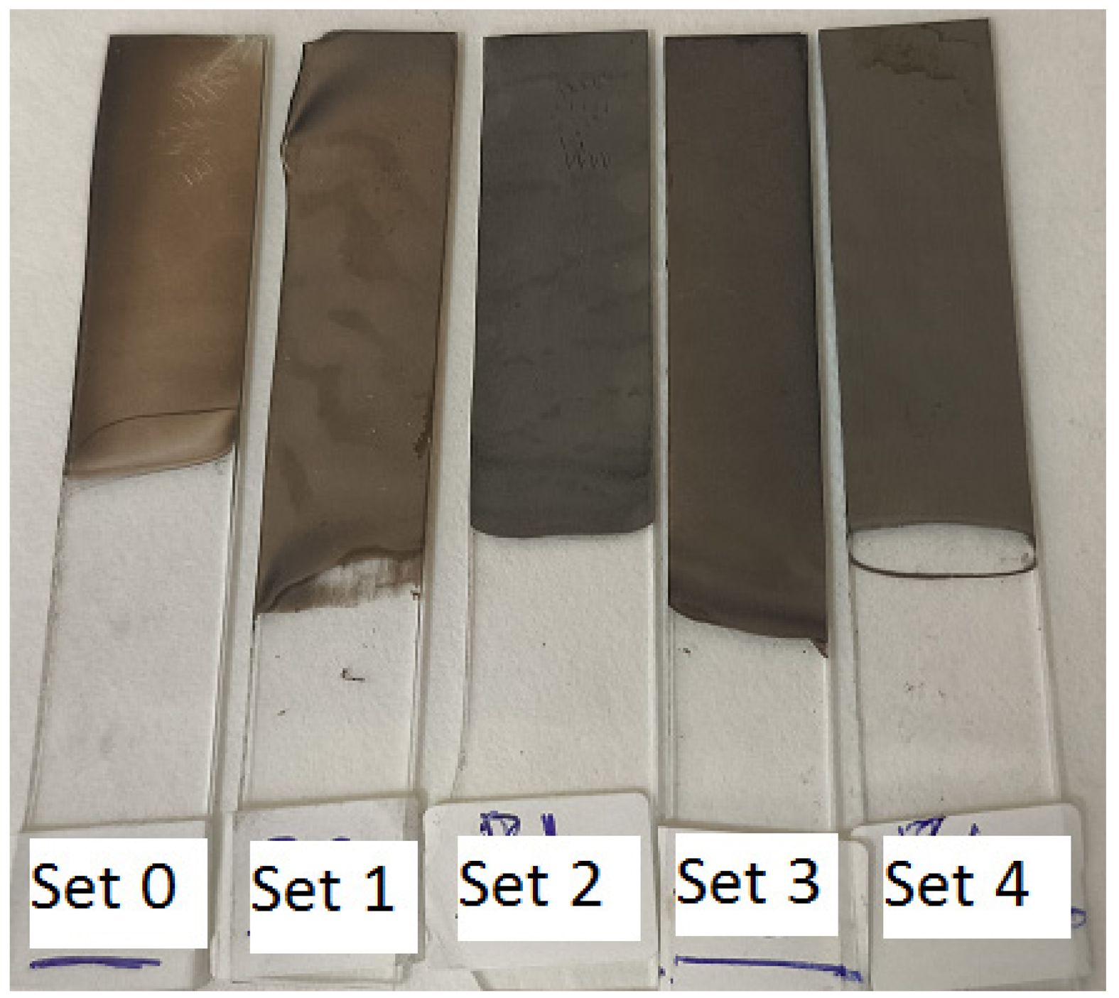
When the images in Fig. 7 are examined, it is seen that the films are coated homogeneously onto the glass substrate. It is assumed that the darkness on the film surface obtained in Set 2 arises due to the relatively high thickness of the film, which is 2955 nm. Furthermore, it is noticeable that all of the films were coated quite homogeneously and smoothly on their surfaces. No defects are observed on the sample surfaces, especially those using 15 mg and 20 mg inhibitors.
|
Fig. 1 PbSe film thicknesses measured using SEM. |
|
Fig. 2 XRD patterns of PbSe films. |
|
Fig. 3 SEM images of PbSe films at 50 kx magnification. |
|
Fig. 4 Elemental analysis results of PbSe films obtained from EDX. |
|
Fig. 5 Surface roughness images of PbSe films obtained from ImageJ software. |
|
Fig. 6 Surface resistivity results of PbSe films measured by the four-probe method. |
|
Fig. 7 Photo of PbSe films. |
In my study, PbSe films were produced using CBD. The effects of using an inhibitor (Na₂SO₃) in the production of PbSe films were investigated for the first time. In addition to the chemicals Pb(NO₃)₂, TEA, NH₃, and CSe(NH₂)₂ used to form the precursor solution, 5 to 20 mg of Na₂SO₃ was added to decrease the reaction rate. It has been observed that incorporating inhibitors is effective, leading to an enhancement in film thickness by up to 3.5 times. XRD analysis indicated that all films formed in a cubic crystal structure, and the use of an inhibitor reduced the crystallite size and increased the dislocation density value. SEM images indicate that all film surfaces were uniformly coated. The morphology of the films was noted to transform into a cauliflower-like structure as a result of the application of inhibitors. It was also calculated that the use of an inhibitor reduced the films’ average surface roughness from 27 nm to 17 nm. According to the EDX analysis of the films, the Se/Pb ratio was observed to approach 1 in correlation with the rise in inhibitor content. Surface resistivity values obtained with the four-probe method also revealed that the use of an inhibitor increased them up to 30 times. The tone change in the photographs of the films is an indication of the change in film thickness and the homogeneous coating of the glass substrate.
This research received no external funding.
The author declares that I have no known competing financial interests or personal relationships that could have appeared to influence the work reported in this paper.
Data will be made available on reasonable request.
Not Applicable
- 1. F. Kipgen, L.R. Singh, P.J. Saikia, S.R. Devi, and M.A. Hussain, Next Mater. 9 (2025) 101009.
-

- 2. P.O. Isi, K. Emumejaye, O.A. Ikenga, C.B. Muomeliri, C.E. Uzor, and J. Isah, J. Basic Phys. Res 14[1] (2025) 61-68.
- 3. C.A. Rodríguez, A.C. Mera, L. Pizarro-Castillo, M. Ashfaq, M.G. Sandoval-Paz, M.J. Cortés Burgos, P. Manidurai, and S. Suárez, Mater. Sci. Semicond. Process. 131 (2021) 105839.
-
- 4. Y. Liu, L.L. McDowell, L. Su, Y. Luo, J. Qiu, and Z. Shi, Mater. Sci. Semicond. Process. 150 (2022) 106963.
-
- 5. S. Peng, H. Li, C. Zhang, J. Han, X. Zhang, H. Zhou, X. Liu, and J. Wang, Nanomaterials 12[9] (2022) 1391.
-
- 6. J.T. Harrison and M.C. Gupta, J. Alloys Compd. 905 (2022) 164155.
-
- 7. A. Wang, S. Bao, M. Zhao, X. Sun, and L. Shi, Integr. Ferroelectr. 240 (2024) 506-516.
-
- 8. S. Abel, J.L. Tesfaye, L. Gudata, F. Lamessa, R. Shanmugam, L.P. Dwarampudi, N. Nagaprasad, and R. Krishnaraj, J. Nanomater. 2022 (2022) 3108506.
-
- 9. S. Roa, M. Sandoval, and M. Sirena, Mater. Chem. Phys. 264 (2021) 124479.
-
- 10. S. Roa, M. Sandoval, and S. Suárez, Solid State Sci. 113 (2021) 106545.
-
- 11. L.N. Maskaeva, V.M. Yurk, V.F. Markov, M.V. Kuznetsov, V.I. Voronin, R.D. Muhamediarov, and G.V. Zyrianov, Mater. Sci. Semicond. Process. 108 (2020) 104867.
-
- 12. S. Anwar, M. Pattanaik, B.K. Mishra, and S. Anwar, Mater. Sci. Semicond. Process. 34 (2015) 45-51.
-
- 13. G.G. Ali and T.A. Aswad, J. Univ. Anbar Pure Sci. 17 (2023) 225-233.
-
- 14. J.I. Contreras-Rascón, J. Díaz-Reyes, A. Flores-Pacheco, R. Lozada Morales, M.E. Álvarez-Ramos, and J.A. Balderas-López, Results Phys. 22 (2021) 103914.
-
- 15. F.G. Hone and F.K. Ampong, Mater. Chem. Phys. 183 (2016) 320-325.
-
- 16. S. Anwar, S. Anwar, and B.K. Mishra, Mater. Sci. Semicond. Process. 40 (2015) 910-916.
-
- 17. A. Wang, S. Bao, M. Zhao, X. Sun, and L. Shi, Integr. Ferroelectr. 240[3] (2024) 506-516.
-
- 18. I.A. Kariper, Surf. Rev. Lett. 27[7] (2020) 1950175.
-
- 19. B. Altiokka, M.C. Baykul, and M.R. Altiokka, J. Cryst. Growth 384 (2013) 50-54.
-
- 20. B. Altıokka, Arab. J. Sci. Eng. 40 (2015) 2085-2093.
-
- 21. B. Altıokka, J. Electron. Mater. 48 (2019) 2398-2403.
-
- 22. M. Önal and B. Altiokka, Acta Phys. Pol. A 143[5] (2023) 355-361.
-
- 23. V.M. Yurk, L.N. Maskaeva, V.F. Markov, and V.G. Bamburov, Russ. J. Appl. Chem. 92 (2019) 394-403.
-
- 24. K.A. Nordquist, K.M. Schaab, J. Sha, and A.H. Bond, Cryst. Growth Des. 17 (2017) 4049-4055.
-
- 25. T.J. Malek, S.H. Chaki, R.K. Giri, and M.P. Deshpande, Appl. Phys. A Mater. Sci. Process. 128 (2022) 1.
-
- 26. M. Narasimha Murthy, C.J. Sreelatha, G. Ravinder, and S. Anusha, Mater. Today Proc. 54 (2022) 602-607.
-
- 27. T. Vigneswari and P. Raji, J. Ceram. Process. Res. 17 (2016) 999-1005.
-
- 28. S. Shanmugan, D. Mutharasu, P. Anithambigai, N. Teeba, and I. Abdul Razak, J. Ceram. Process. Res. 14 (2013) 385-390.
-
- 29. F. Saadaoui, A. Rjeb, B. Akharkhach, A. Nfissi, and S. Sayouri, J. Ceram. Process. Res. 20 (2019) 139-142.
-
- 30. M. Önal and B. Altıokka, Emerg. Mater. Res. 9 (2020) 738-742.
-
- 31. M.C. Gupta, J.T. Harrison, and M.T. Islam, Mater. Adv. 2 (2021) 3133-3160.
-
- 32. N.A. Bakr, Z.T. Khodair, and A.M. Saleh, 13 (2018) 10796.
- 33. S. Dev, P. Kumar, A. Rani, A. Agarwal, and R. Dhar, Superlattices Microstruct. 145 (2020) 106638.
-
- 34. S.J. Ikhmayies, Jom 73 (2021) 1261-1270.
-
- 35. M. Önal, Jom 77 (2025) 6521-6529.
-
 This Article
-
2026; 27(1): 89-95
Published on Feb 28, 2026
- 10.36410/jcpr.2026.27.1.89
- Received on Sep 23, 2025
- Revised on Jan 3, 2026
- Accepted on Jan 8, 2026
Services
- Abstract
introduction
experimental details
results and discussion
conclusions
- Acknowledgements
- Conflict of Interest
- Data availability statement
- Ethical approval
- References
- Full Text PDF
Shared
Correspondence to
- Metehan Önal
-
Bilecik Seyh Edebali University, Bilecik, 11210, Turkey
Tel : +902282141596, +905558727182 Fax: +902282141332 - E-mail: metehan.onal@bilecik.edu.tr
Clean-Energy Research Institute(CRI), Hanyang University, 222, Wangsimni-ro, Seongdong-gu, Seoul, 04763, Korea
E-mail: jcpr@hanyang.ac.kr