


- Epitaxial growth and phase stabilization of κ-Ga₂O₃ on GaN templates via metal-organic chemical vapor deposition
Dong Ho Leea, Jung-Bok Leeb, Seon Jin Muna, Hyung Soo Ahna and Min Yanga,*
aDepartment of Nano Semiconductor Engineering, Korea Maritime and Ocean University, Busan 49112, Korea
bDepartment of Electrical Engineering, Pusan National University, Busan 46241, KoreaThis article is an open access article distributed under the terms of the Creative Commons Attribution Non-Commercial License (http://creativecommons.org/licenses/by-nc/4.0) which permits unrestricted non-commercial use, distribution, and reproduction in any medium, provided the original work is properly cited.
In this study, κ-Ga₂O₃ thin films were heteroepitaxially grown on GaN templates using metal-organic chemical vapor deposition (MOCVD), and the effects of growth conditions and nucleation layer structures on phase formation and crystalline quality were systematically investigated. Under direct growth conditions, increasing the growth temperature and H₂O flow rate led to the incorporation of the β-Ga₂O₃ phase. In particular, mixed κ + β phases were observed at elevated temperatures above 680 °C. To suppress β-phase formation and maintain a single κ phase, a two-step growth method was employed, and the influence of nucleation layer thickness and structure on the crystalline quality was comparatively analyzed. As a result, the 100 nm-thick κ-Ga₂O₃ nucleation layer exhibited improved surface coalescence and a reduced threading dislocation density, effectively suppressing β-phase formation even under high-temperature epitaxial conditions. Φ-scan analysis further confirmed the presence of three-fold rotational domains in the κ-Ga₂O₃ films and revealed an in-plane epitaxial relationship of κ-Ga₂O₃ (201) // GaN (11-20). Additionally, the maximum growth temperature at which a single-phase κ-Ga₂O₃ could be maintained was identified to be 720 °C. These findings propose an effective approach for the stable growth of single-phase κ-Ga₂O₃ thin films at elevated temperatures.
Keywords: MOCVD, Ga2O3, Crystal phase, Structural evolution, GaN/Si template.
Gallium oxide (Ga₂O₃), a semiconductor with an ultrawide bandgap of 4.5-5.3 eV, has emerged as a promising candidate for next-generation power electronics, and has attracted considerable research interest in recent years. Ga₂O₃ exists in various polymorphs including α, β, γ, δ, and κ (also known as ε), each exhibiting distinct physical properties and phase stability depending on the processing conditions and temperature [1, 2]. Among them, β-Ga₂O₃ with a monoclinic structure (space group C2/m) is the most thermodynamically stable phase. With its wide bandgap (~4.9 eV) and high breakdown electric field (~8.0 MV/cm), it has been extensively investigated in various applications, ranging from high-power devices and nanostructured forms such as hollow particles and nanowires [3-6]. To obtain single crystalline β-Ga₂O₃ substrates, various bulk growth methods such as the Czochralski method, edge defined film fed growth (EFG), and Bridgman process have been investigated, and the achievable wafer size has been steadily increasing. Recently, the successful growth of β-Ga₂O₃ wafers up to 6 inches in diameter has been reported [7-9].
On the other hand, the metastable κ-phase of Ga₂O₃ has attracted attention due to its unique physical characteristics. κ-Ga₂O₃ belongs to the orthorhombic Pna2₁ space group, with an in-plane lattice constant ratio of a:b = 1:√3 [10, 11]. This structural configuration allows for excellent lattice compatibility with hexagonal symmetry substrates, including sapphire, SiC, GaN, and Si(111). Furthermore, κ-Ga₂O₃ possesses a large spontaneous polarization coefficient (PSP ~ 0.23 C/m²), which is significantly higher than that of GaN (0.029-0.034 C/m²). As a result, κ-Ga₂O₃ can induce a high-density two-dimensional electron gas (2DEG) at the heterojunction interface even without intentional doping, offering a new pathway for high-electron-mobility transistor (HEMT) development [10, 12-14]. For instance, Wang et al. demonstrated that ε-Ga₂O₃/m-GaN(AlN) heterojunctions can achieve 2DEG densities exceeding 10¹⁴ cm⁻² without doping [16]. Additionally, ε-Ga₂O₃ has been reported to exhibit ferroelectricity, and its dielectric constant (~32 at 10 kHz) is comparable to those of high-k dielectrics such as HfO₂ and La₂O₃ [15].
These attributes make κ-Ga₂O₃ highly attractive for high-performance heterostructure devices with III-nitride semiconductors. Despite its potential, most previous studies on κ-Ga₂O₃ thin film growth have utilized common substrates such as Si or sapphire and have also employed SiC substrates to address the inherent low thermal conductivity of Ga₂O₃ [17-20]. Given its importance, the heteroepitaxial growth of κ-Ga₂O₃ on GaN remains relatively underexplored. Moreover, since most GaN templates are based on sapphire substrates, they suffer from poor thermal dissipation, which limits their applicability in device fabrication [33, 34]. To overcome these challenges, this study explores the heteroepitaxial growth of κ-Ga₂O₃ on a GaN/Si template via metal-organic chemical vapor deposition (MOCVD), aiming to simultaneously maximize the material's intrinsic properties and improve thermal management in potential device applications.
Several critical issues remain in κ-Ga₂O₃ epitaxy. One such challenge is the presence of rotational domains during growth. Due to its orthorhombic structure, κ-Ga₂O₃ tends to form hexagonally symmetric islands based on threefold rotational symmetry, leading to the formation of grain boundaries. These rotational domains can generate various types of defects, such as charge trapping states and leakage current paths [21]. They also degrade the alignment uniformity and increase dislocation density [20]. These problems can be mitigated by employing epitaxial lateral overgrowth (ELOG) techniques [22-24], and recent studies suggest that ε-GaFeO₃ substrates can help suppress in-plane rotational domains [25, 26]. Another major challenge is that bulk κ-Ga₂O₃ is of limited availability, thus requiring heteroepitaxy for device applications. Among the various growth parameters, temperature plays a dominant role in determining phase formation. In most MOCVD based reports, κ-Ga₂O₃ is formed at temperatures up to ~700 °C [27]. Furthermore, lattice mismatch with the substrate often leads to the nucleation of β-Ga₂O₃, resulting in phase mixtures that hinder the realization of pure κ-phase properties. To address this, efforts have been made to optimize substrate selection, growth pressure, precursor ratios (VI/III), and temperature conditions to achieve phase-pure κ-Ga₂O₃ [28-32]. Nevertheless, temperature remains a particularly sensitive factor, with many studies reporting mixed κ+β phases or even full phase transitions to β-Ga₂O₃ at temperatures above 700 °C, effectively limiting the upper bound for MOCVD process temperatures.
In this study, we employed both direct and two-step growth approaches via MOCVD to deposit κ-Ga₂O₃ thin films on GaN/Si templates. Initially, optimal growth conditions were identified through direct growth experiments, and the influence of various growth parameters on phase formation was analyzed. Subsequently, these findings were applied to a two-step process, where a nucleation layer was introduced to suppress β-phase formation. Our results confirmed that the κ-phase nucleation layer effectively inhibited β-phase crystallization, enabling phase-pure κ-Ga₂O₃ growth even at elevated temperatures up to 720 °C. These findings demonstrate that the two-step MOCVD approach is effective for suppressing β-Ga₂O₃ nucleation and achieving single-phase κ-Ga₂O₃ thin films under high temperature conditions.
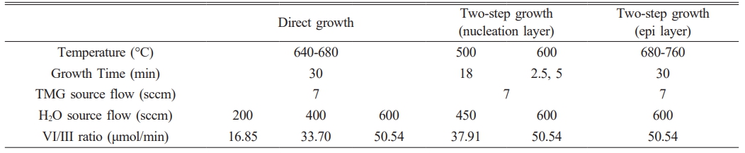
Ga₂O₃ thin films were epitaxially grown on GaN templates using a custom-built horizontal metal-organic chemical vapor deposition (MOCVD) system. The GaN template employed in this study was designed as a multilayer structure to ensure high crystalline quality. From bottom to top, the layer stack comprised a Si(111) substrate, a 200 nm AlN buffer layer, 1500 nm AlGaN/AlN superlattices (SLs), a 600 nm u-GaN, a 5 nm AlN, and a 1200 nm u-GaN top layer. The crystalline quality of the GaN template was confirmed by high-resolution X-ray diffraction (HRXRD), where the full width at half maximum (FWHM) of the GaN (002) rocking curve was measured to be approximately 1.3°. Trimethylgallium (TMG) was used as the Ga precursor and maintained at −10 °C. Ultra-pure deionized H₂O served as the oxygen precursor and was kept at room temperature. High-purity (6N) nitrogen (N₂) was used as the carrier gas. All growth processes were performed under atmospheric pressure. The TMG flow rate was fixed at 7 sccm (17.05 μmol/min) throughout all experiments. The single-step growth process is referred to as direct growth, where the Ga₂O₃ thin film was deposited directly on the GaN surface. Growth temperatures were varied from 640 to 680 °C in 20 °C intervals, with a fixed growth time of 30 min. The two-step growth process involved a nucleation step followed by an epitaxial growth step. In the nucleation step, Ga₂O₃ films were grown under three different conditions with varying temperatures and thicknesses. In the second step, the epitaxial growth was carried out for 30 min at temperatures ranging from 680 to 760 °C in 20 °C increments. Detailed process parameters are summarized in Table 1. The crystal structure and phase composition of the grown films were evaluated by high-resolution X-ray diffraction (HRXRD, RIGAKU) using a two-bounce Ge(220) monochromator with Cu Kα₁ radiation. Phase identification was performed via 2θ-ω scans, while crystal quality and threading dislocation density were evaluated using ω-scans (rocking curves). The crystallographic orientation and in-plane alignment were investigated using azimuthal (Φ-scan) measurements. Surface morphology and film thickness were characterized using field emission scanning electron microscopy (FE-SEM, Tescan CLARA). Atomic force microscopy (AFM, Park Systems) was employed to evaluate the surface roughness and growth mode of the films.
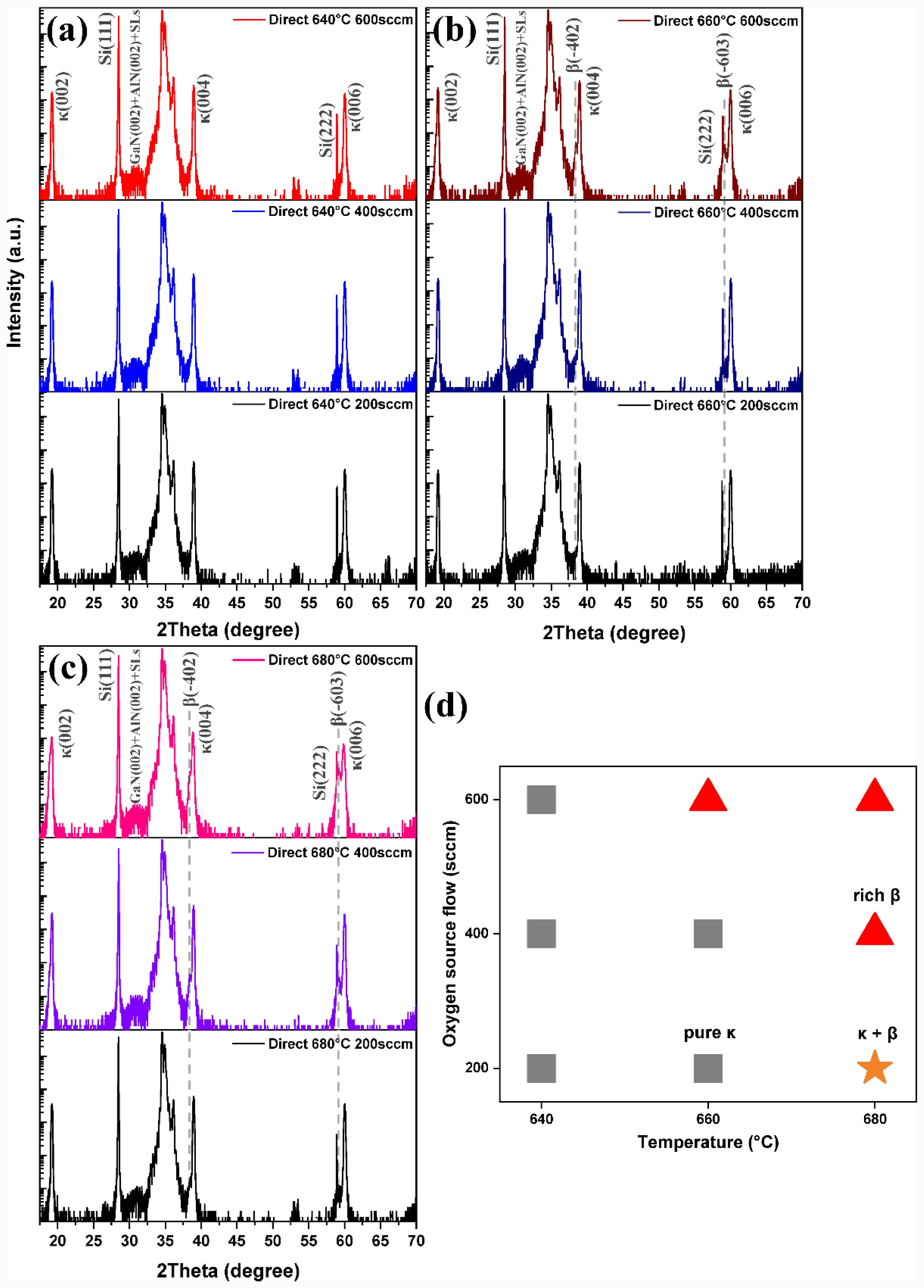
To investigate the phase evolution of Ga₂O₃ thin films under various growth conditions, XRD analysis was performed. In order to evaluate the tendency of β-Ga₂O₃ phase formation as a function of H₂O flow rate within the thermal window where κ-Ga₂O₃ is thermodynamically stable, Fig. 1(a) presents the XRD pattern of the sample grown at 640 °C under direct growth. A dominant single-phase κ-Ga₂O₃ structure was observed, with strong preferential orientations along the (002) (19.20°), (004) (38.96°), and (006) (60.02°) planes. As shown in Fig. 1(b), at 660 °C, the κ-Ga₂O₃ single-phase was maintained at H₂O flow rates of 200 and 400 sccm. However, upon increasing the H₂O flow to 600 sccm, peaks corresponding to β-Ga₂O₃ began to emerge. In particular, the (-201) reflection of β-Ga₂O₃ (18.9°) is nearly overlapped with the κ-Ga₂O₃ (002) peak (19.2°), making them indistinguishable in peak separation. Instead, peak broadening of the κ-Ga₂O₃ (002) peak was observed, and distinct β-Ga₂O₃ peaks at (-402) (38.4°) and (-603) (59.17°) were clearly detected. Fig. 1(c) shows the XRD pattern of a sample grown at 680 °C. At a lower H₂O flow rate of 200 sccm, β-Ga₂O₃ appeared as shoulder peaks overlapping with the κ-Ga₂O₃ reflections. As the H₂O flow rate increased to 400 and 600 sccm, β-Ga₂O₃ (-402) and (-603) peaks became more pronounced, and further broadening of the κ-Ga₂O₃ (002) peak was observed. The phase diagram in Fig. 1(d) summarizes the observed phase evolution under direct growth conditions. Growth conditions yielding pure κ-Ga₂O₃ phase are marked as gray squares, conditions showing partial β-Ga₂O₃ presence as shoulders are shown as orange stars, and conditions with fully resolved β-Ga₂O₃ peaks are represented by red triangles. These results indicate that growth temperature is the most critical factor governing β-Ga₂O₃ formation, consistent with previous reports [28, 32]. Furthermore, under fixed temperature conditions, an increase in H₂O flow rate was found to promote the coexistence of the β-Ga₂O₃ phase.
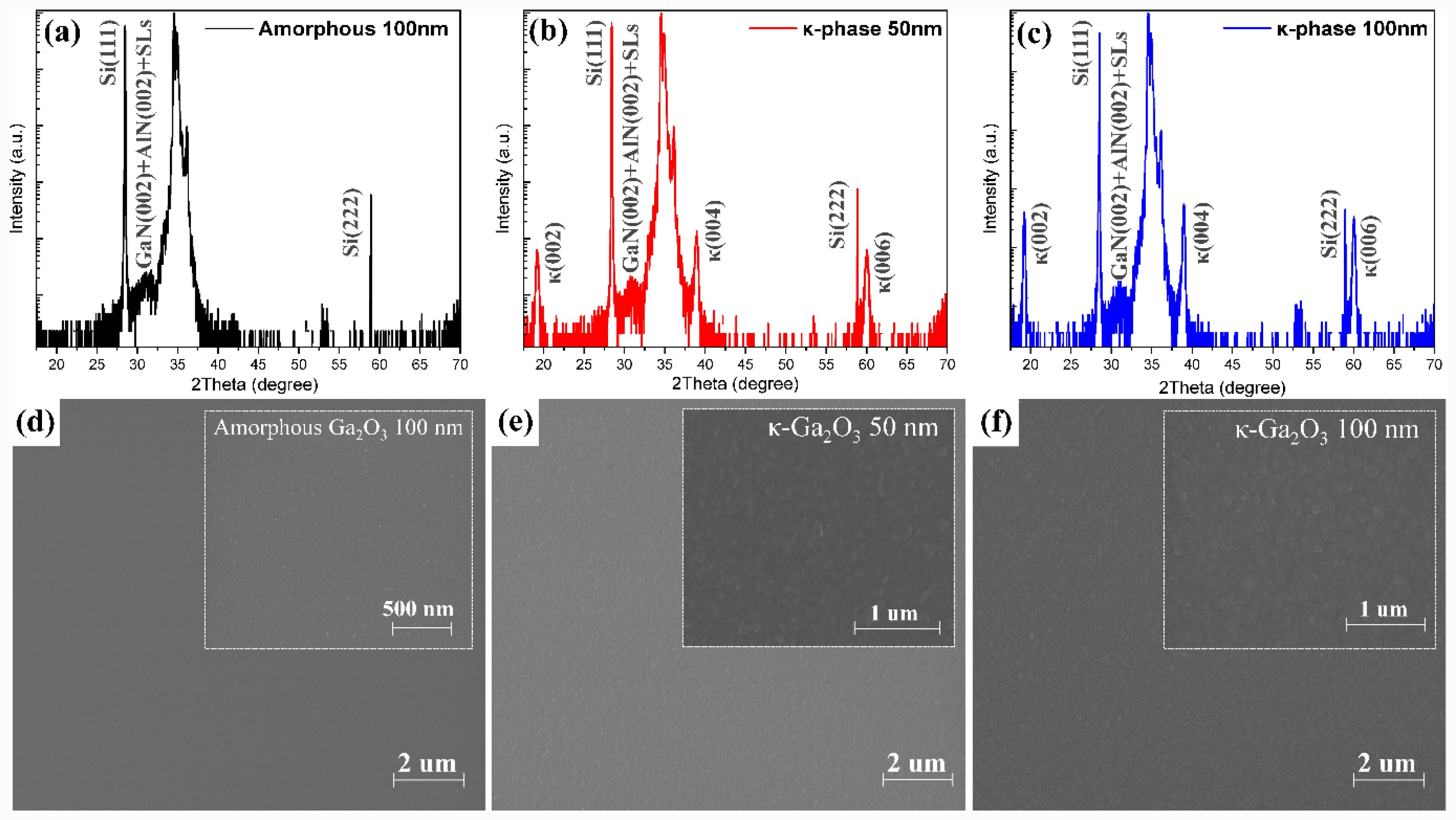
In heteroepitaxy, the two-step growth method is considered an effective approach to relieve lattice stress between the substrate and the film and to enable the growth of high-quality thin films. This technique, consists of a low temperature nucleation layer and a high temperature epitaxial layer, has been widely adopted for the growth of high-quality nitrides and oxides [29, 35, 36]. Previous studies have reported that during the initial growth stage of κ-Ga₂O₃ a thin transition layer or β-Ga₂O₃ nuclei tend to form [27, 28, 49]. This behavior is attributed to the initial stress caused by lattice mismatch between the substrate and the film under high growth temperatures. The resulting transition layer can be regarded as a structural accommodation that relieves interfacial strain. This early phase mixing often persists throughout the entire growth, leading to κ+β mixed-phase films. Therefore, it is crucial to suppress β-phase nucleation during the nucleation stage to achieve single-phase κ-Ga₂O₃ epitaxy. To address this, we systematically investigated the effect of different types and thicknesses of nucleation layers on the resulting film structure. Specifically, we prepared amorphous and crystalline κ-Ga₂O₃ nucleation layers with different thicknesses (50 and 100 nm) on GaN templates, followed by subsequent film growth. As shown in Fig. 2(a), the Ga₂O₃ film deposited at 500 °C exhibited no identifiable diffraction peaks. Consistently, the corresponding SEM image Fig. 2(d) revealed a very smooth surface composed of randomly oriented fine particles, confirming the formation of an amorphous nucleation layer at this temperature [37]. To stabilize single-phase κ-Ga₂O₃ and suppress β-phase formation, the nucleation temperature was set to 600 °C. When the κ-Ga₂O₃ layer was grown to a thickness of 50 nm Fig. 2(b), weak κ-phase peaks were observed, although the intensity was relatively low. In the SEM image of Fig. 2(e), the surface appeared very rough, the thin film was not sufficiently coalesced, and the grain arrangement was found to be disordered. In general, during the initial nucleation stage in the two-step growth method, the film grows in a three-dimensional (3D) mode [38]. In addition, according to the study by Narayanan et al., faulted regions formed in the nucleation layer act as one of the main sources of threading dislocations (TDs) [39]. In our case, the 50 nm nucleation layer appeared insufficient to suppress TD formation, leading to polycrystalline characteristics. On the other hand, as shown in Fig. 2(c), increasing the nucleation layer thickness to 100 nm resulted in the appearance of well defined κ-Ga₂O₃ diffraction peaks with enhanced intensity. The SEM image in Fig. 2(f) shows that the surface is smoother than that of the 50 nm condition, with reduced 3D island structures and a more ordered grain arrangement. This can be attributed to the fact that, as the thickness of the nucleation layer increases, surface coalescence is promoted, which is generally associated with improved crystal quality.
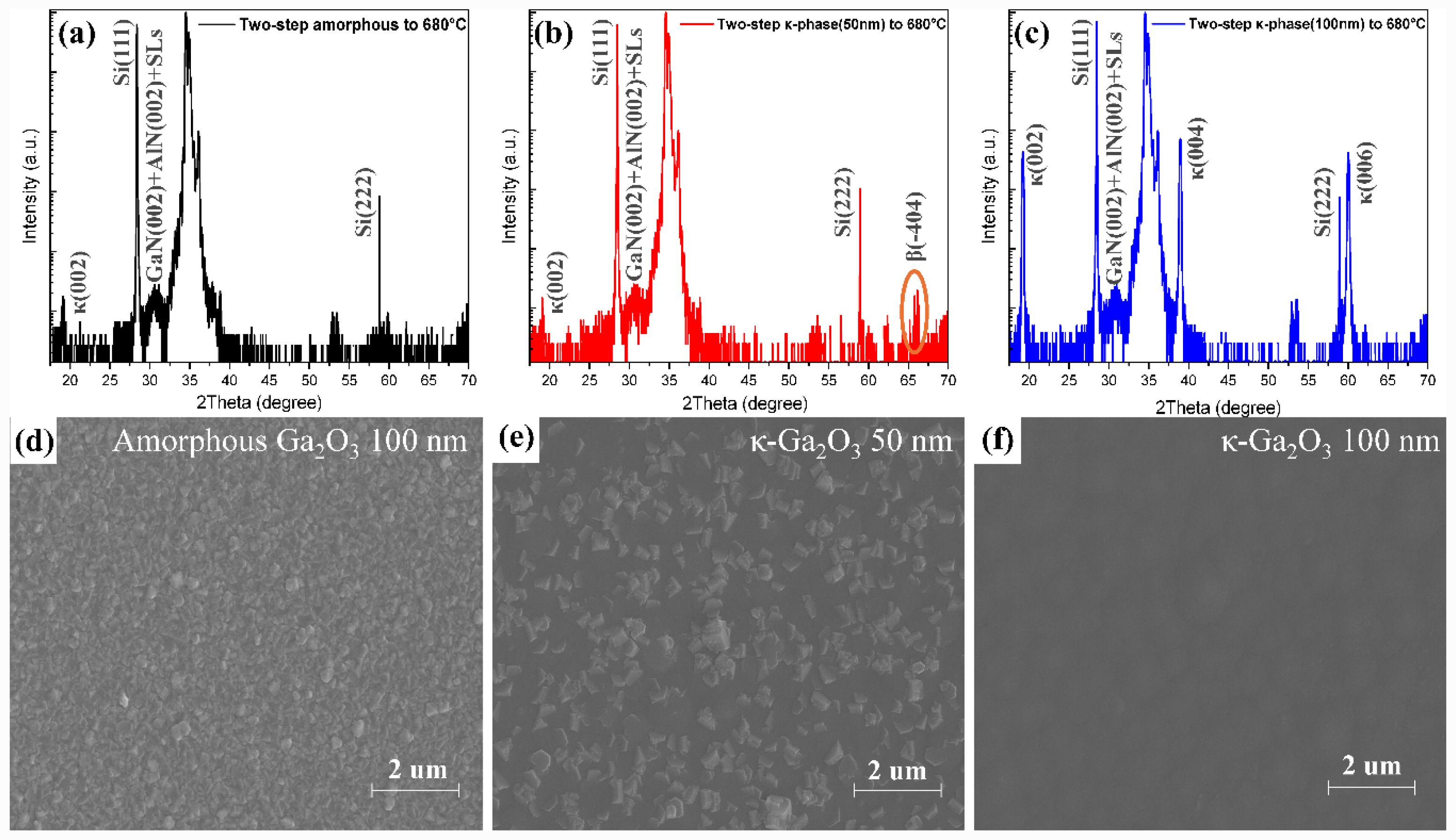
Based on the nucleation layer results in Fig. 2, Two-step epitaxial growth was performed under the same conditions (680 °C, H₂O: 600 sccm) that led to significant β-phase formation in the direct growth process, as shown in Fig. 1. Fig. 3(a) and (d) show the results for the sample grown on an amorphous Ga₂O₃ nucleation layer. Despite being processed under conditions favorable for κ-phase formation, XRD analysis revealed no Ga₂O₃ related diffraction peaks. SEM imaging revealed a rough surface with highly disordered, random grain orientations. These findings suggest that the amorphous buffer layer disordered structure significantly disrupted the subsequent epitaxial growth. Fig. 3(b) and (e) display the data for the sample grown on a 50 nm thick κ-Ga₂O₃ nucleation layer. The XRD and SEM results were similar to those of the amorphous buffer layer sample, indicating continued disorder in the overgrown film. The limited suppression of threading dislocations by the thin nucleation layer led to disordered crystal orientation, which persisted after epitaxial growth, resulting in a rough and randomly textured surface. A weak peak, likely corresponding to β-Ga₂O₃ (-404), was detected (marked by the orange circle), suggesting phase instability possibly triggered by the structural disorder. Fig. 3(c) and (f) correspond to the film grown on a 100 nm thick κ-Ga₂O₃ nucleation layer. SEM analysis confirmed a smoother surface morphology than the other two cases, indicative of improved crystallographic alignment and uniform growth. Furthermore, no β-Ga₂O₃ peaks were observed in the XRD spectra, and single-phase κ-Ga₂O₃ was maintained. These results demonstrate that, despite the growth conditions being favorable for β-phase formation, the use of a well formed κ-Ga₂O₃ nucleation layer grown via a two-step process effectively suppressed β-phase incorporation, enabling the formation of single-phase κ-Ga₂O₃ films.
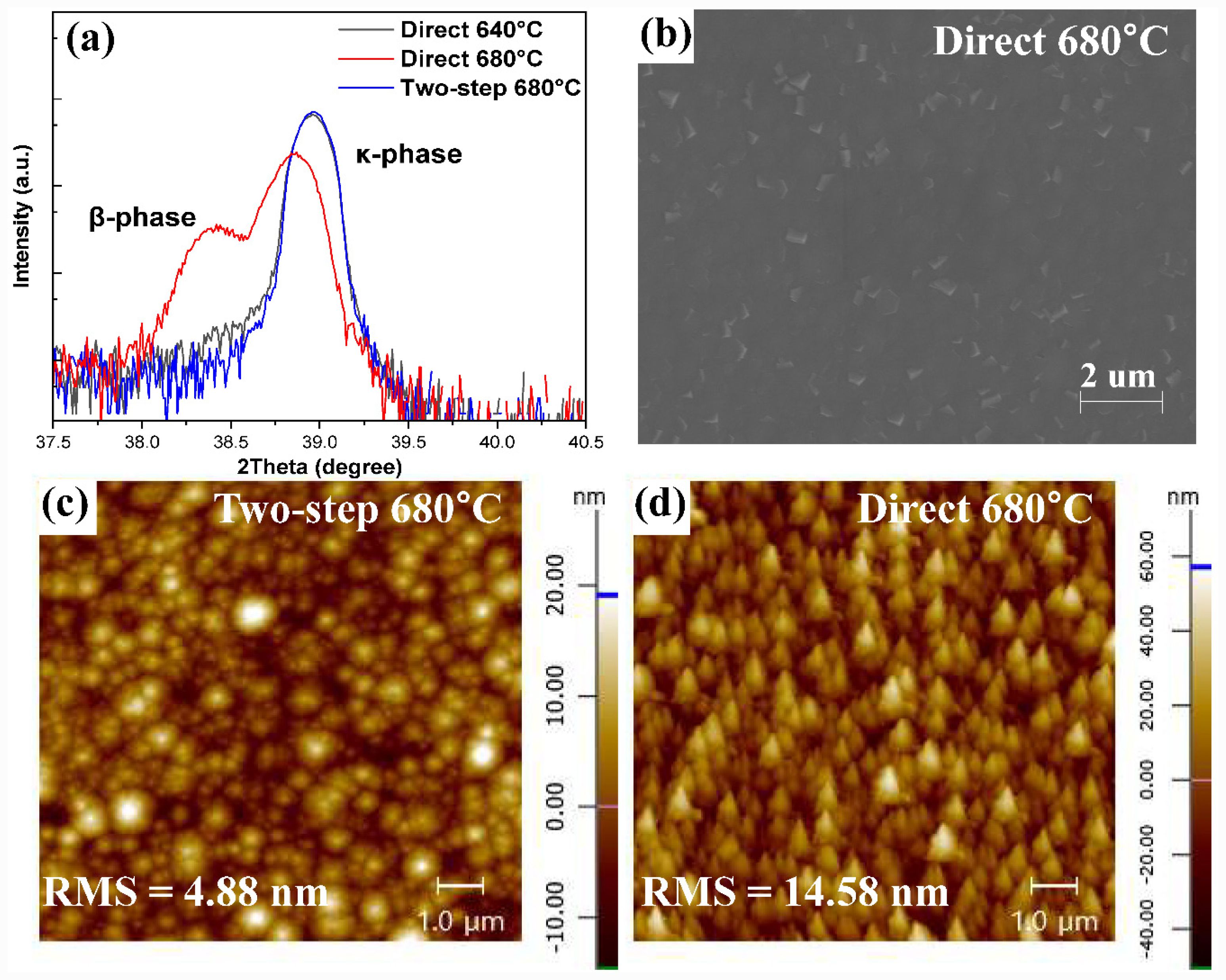
XRD, SEM, and AFM analyses were performed to compare the degree of β-Ga₂O₃ incorporation and surface morphology depending on the growth method. Fig. 4(a) shows a magnified view of the κ-Ga₂O₃ (004) peak in the 2θ-ω scan. While maintaining a constant H₂O flow rate of 600 sccm, the formation of β-Ga₂O₃ phases was compared across different growth temperatures and methods. Under the direct growth method at 640 °C, a single κ-Ga₂O₃ phase was observed, with no detectable β-Ga₂O₃ peaks. In contrast, the direct growth sample grown at 680 °C showed a clear coexistence of κ-Ga₂O₃ and β-Ga₂O₃ phases. Notably, a leftward shift in the κ-Ga₂O₃ (004) peak was observed, attributed to compressive strain at the κ-Ga₂O₃ grain boundaries, induced by β-Ga₂O₃ phase incorporation. Analysis of the c-axis lattice constant revealed that the single-phase κ-Ga₂O₃ sample had a c-axis length of 9.24 Å, while the mixed-phase sample exhibited a slightly larger value of 9.26 Å, an increase of approximately 0.22%, indicating lattice distortion. In contrast, the two-step 680 °C sample showed no significant β-Ga₂O₃ related peaks. Even at the (-402) β-Ga₂O₃ position, the intensity was lower than that of the direct 640 °C sample, suggesting that the formation of a nucleation layer in the two-step process effectively suppressed β-Ga₂O₃ phase formation, even under high-temperature growth conditions. This trend was also evident in surface morphology analysis. The SEM image of the two-step 680 °C sample (shown in Fig. 3(f)) displayed a relatively smooth and uniform surface. On the other hand, the direct 680 °C sample exhibited a mixture of monoclinic β-Ga₂O₃ microcrystals and orthorhombic κ-Ga₂O₃ domains with threefold symmetry. This indicates that in the direct growth method, β-Ga₂O₃ formed not only during nucleation but also during the high-temperature epitaxial growth stage. AFM analysis further confirmed these findings. Fig. 4(c) and (d) show the surface morphologies of the two-step and direct growth samples, respectively. The two-step sample exhibited a Volmer-Weber growth mode with an RMS roughness of 4.88 nm, indicating a relatively smooth surface. In contrast, the direct growth sample showed a much rougher surface, with an RMS value of 14.58 nm, featuring sharp β-Ga₂O₃ microstructures.
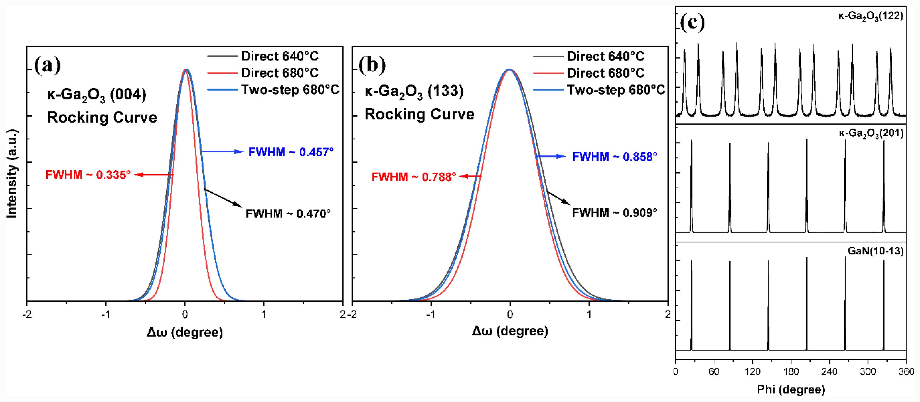
Fig. 5(a) and (b) present the rocking curve results for the κ-Ga₂O₃ (004) and (133) planes. According to the 2θ-ω scan data shown previously in Fig. 4, the full width at half maximum (FWHM) of the κ-Ga₂O₃ (004) peak was measured to be 0.195° for direct 640 °C, 0.223° for direct 680 °C, and 0.190° for two-step 680 °C samples. In contrast, the rocking curve measurements exhibited generally larger FWHM values, which were 0.470° for direct 640 °C, 0.335° for direct 680 °C, and 0.457° for two-step 680 °C. These broader values can be attributed to the formation of mosaic domains typically observed during heteroepitaxial growth, which induce out-of-plane tilt and in-plane twist of the lattice, thereby degrading overall crystalline alignment. The rocking curve method reflects this mosaic spread and thus tends to yield larger FWHM values than the 2θ-ω scans [40]. In this study, the GaN templates used were composed of multilayered structures, and it is presumed that the curvature of the substrate, combined with the large lattice mismatch (~8.8%) between κ-Ga₂O₃ and GaN contributed to the significant mosaic spread. Interestingly, the FWHM values of the single-phase κ-Ga₂O₃ samples (direct 640 °C and two-step 680 °C) were similar, whereas the mixed-phase (β + κ) sample grown at direct 680 °C showed a relatively smaller FWHM. This seemingly counterintuitive result has also been reported in previous studies. For example, S. H. Cho et al. observed that when the nucleation layer was composed of a β + κ mixed-phase, grain competition during subsequent epitaxial growth facilitated the formation of highly aligned κ-Ga₂O₃ films [41]. Similarly, S. Chen et al. reported that in the presence of a β + κ mixed-phase, β-Ga₂O₃ grains acted similarly to the masks in epitaxial lateral overgrowth (ELOG), promoting the lateral growth of κ-Ga₂O₃ grains [11]. Therefore, the mixed-phase nucleation layer observed in the direct 680 °C sample in this study is interpreted to have acted as a growth guide, where β-Ga₂O₃ crystals facilitated the lateral growth of κ-Ga₂O₃, thereby promoting more aligned κ-Ga₂O₃ growth.
The full width at half maximum (FWHM) values obtained from rocking curve measurements can be qualitatively used to evaluate the dislocation density in the epitaxial film. In particular, the out-of-plane FWHM is closely associated with the screw dislocation density (Nscrew), whereas the in-plane FWHM corresponds to the edge dislocation density (Nedge) [42, 43]. Each dislocation density can be approximately estimated using the following equations,
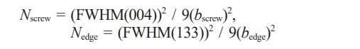
where b is the magnitude of the Burgers vector determined by the lattice parameters of the crystal. For κ-Ga₂O₃, bscrew = 0.291 nm and bedge = 0.926 nm were used in this study [44, 45]. Although a more precise estimation of dislocation densities requires TEM analysis, this study focuses on qualitative and relative comparisons. Based on the calculations, the estimated dislocation densities are as follows,
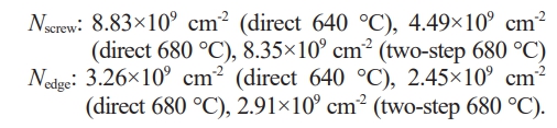
In conclusion, the single-phase κ-Ga₂O₃ samples (direct 640 °C and two-step 680 °C) showed comparable degrees of dislocation densities. However, the mixed-phase (β + κ) sample grown at direct 680 °C exhibited relatively lower dislocation densities. To investigate the epitaxial relationship between κ-Ga₂O₃ and the GaN template, and to examine the presence of rotational domains in κ-Ga₂O₃ thin films, Φ-scan measurements were conducted on samples grown at 680 °C using the two-step growth method. Fig. 5(c) presents the Φ-scan patterns corresponding to the (201) and (122) planes of κ-Ga₂O₃, as well as the (10-13) plane of GaN. The Bragg angles (θ) of these planes were measured to be 18.49° for κ-Ga₂O₃ (201), 16.75° for κ-Ga₂O₃ (122), and 31.73° for GaN (10-13). In the Φ-scan results of κ-Ga₂O₃ (201) and GaN (10-13), six distinct diffraction peaks were observed at 60° intervals, and these peaks overlapped at the same phi positions. This indicates that the two planes are aligned in the same orientation, suggesting an in-plane epitaxial relationship of κ-Ga₂O₃ (201) // GaN (11-20). Additionally, the Φ-scan result for the κ-Ga₂O₃ (122) plane revealed twelve distinct diffraction peaks, indicating that the orthorhombic unit cells of κ-Ga₂O₃ possess three-fold rotational symmetry. These results suggest that the two-step growth method is insufficient to suppress the formation of rotational domains, unlike techniques such as epitaxial lateral overgrowth (ELOG) or the use of ε-GaFeO₃ substrates.
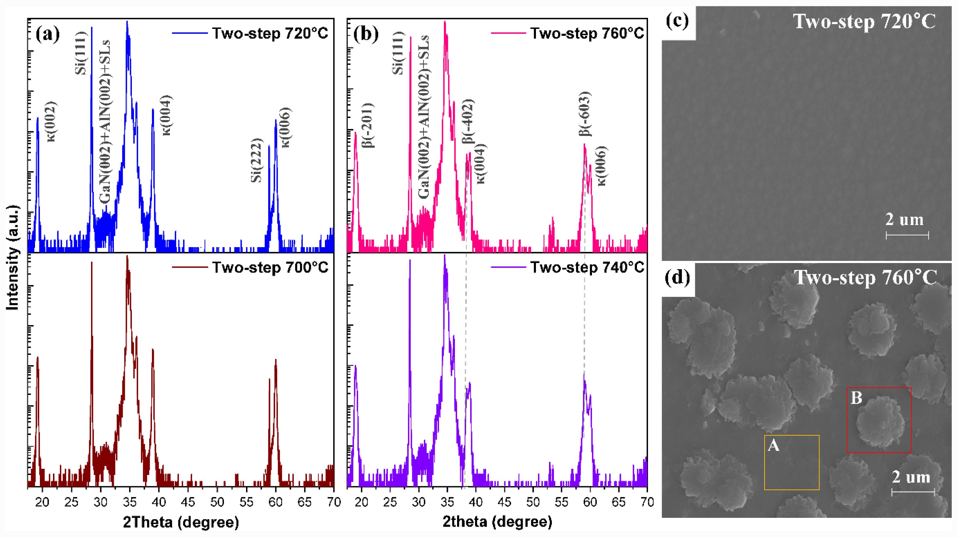
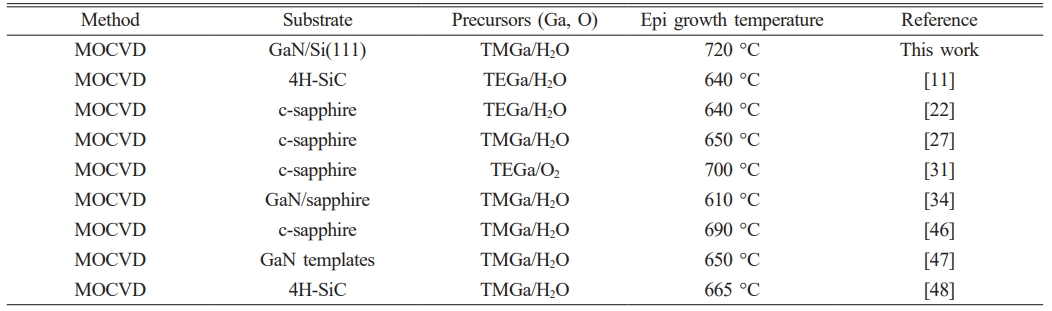
Based on the previous findings that the two-step growth process effectively suppresses the formation of the β-Ga₂O₃ phase during κ-Ga₂O₃ growth, it is necessary to determine the maximum epitaxial growth temperature at which a single-phase κ-Ga₂O₃ film can be maintained. Fig. 6(a) and (b) show the XRD analysis results of samples grown at various epitaxial temperatures ranging from 700 °C to 760 °C, in 20 °C increments. The results confirmed that the single-phase κ-Ga₂O₃ structure was retained up to 720 °C. Representative diffraction peaks within this temperature range appeared at κ-Ga₂O₃ (002) 19.2°, (004) 38.96°, and (006) 60.02°. In contrast, the β-Ga₂O₃ phase was only weakly detected as a shoulder on the lower-angle side of the κ-Ga₂O₃ (006) peak. As summarized in Table 2, the κ-Ga₂O₃ thin film reported in this study was grown at the highest temperature ever reported for a single-phase κ-Ga₂O₃ using the MOCVD process. However, when the growth temperature was increased to 740 °C or higher, a rapid phase transition to β-Ga₂O₃ occurred. The κ-Ga₂O₃ (002) peak at 19.2° disappeared, while a β-Ga₂O₃ (-201) peak emerged at 18.92°. Additional β-Ga₂O₃ (-402) and (-603) peaks also appeared to the left of the κ-Ga₂O₃ (004) and (006) peaks, with intensities comparable to or greater than those of the κ-Ga₂O₃. These findings demonstrate that, through the two-step growth method, single-phase κ-Ga₂O₃ can be achieved even beyond the previously reported thermal stability limit of ~700 °C. To analyze the sample grown at 720 °C, where single-phase κ-Ga₂O₃ was achieved, and to investigate the subsequent phase transition and morphological evolution at higher temperatures, SEM measurements were conducted. Fig. 6(c) presents the SEM result for the sample grown at an epitaxial temperature of 720 °C. The film exhibited a single-phase κ-Ga₂O₃ structure with a relatively smooth surface morphology. Fig. 6(d) presents the SEM image of the sample grown at 760 °C. The image reveals the presence of large island morphologies distributed across the surface, indicating insufficient coalescence between them. In contrast, regions where coalescence had already occurred exhibited relatively flat surface morphologies. This surface morphology can be explained by a mixed-phase formation mechanism. The low grain density of κ-Ga₂O₃ makes it difficult to achieve sufficient coalescence within a short growth period, leading to rough, island-shaped features such as those observed in region B. Conversely, the presence of β-Ga₂O₃ can induce epitaxial lateral overgrowth (ELOG), which promotes the lateral growth of κ-Ga₂O₃ crystals. As a result, relatively smooth surfaces are formed in coalesced areas like region A [11].
|
Fig. 1 (a-c) 2θ-ω scan XRD spectra of Ga₂O₃ thin films directly grown under various temperatures and H₂O flow rates. (d) Phase diagram summarizing κ/β phase evolution under direct growth conditions. |
|
Fig. 2 2θ-ω scan XRD spectra of nucleation layers grown at (a) 500 °C (100 nm), (b) 600 °C (50 nm), and (c) 600 °C (100 nm). (d-f) Corresponding SEM images. |
|
Fig. 3 2θ-ω scan XRD spectra of κ-Ga₂O₃ thin films grown at 680 °C via the two-step method with various nucleation layers. (a) 500 °C (100 nm), (b) 600 °C (50 nm), and (c) 600 °C (100 nm). (d-f) Corresponding SEM images. |
|
Fig. 4 (a) Magnified 2θ-ω scan spectra near the κ-Ga₂O₃ (004) peak for direct 640 °C, direct 680 °C, and two-step 680 °C samples. (b) SEM image of the direct 680 °C sample. (c) and (d) AFM images of the two-step 680 °C and direct 680 °C samples, respectively. |
|
Fig. 5 (a) and (b) Rocking curves of κ-Ga₂O₃ (004) and (133) planes for the direct 640 °C, direct 680 °C, and two-step 680 °C samples. (c) Φ-scan XRD spectra of the κ-Ga₂O₃ (201), (122), and GaN (10-13) planes for the two-step 680 °C sample. |
|
Fig. 6 (a) and (b) 2θ-ω scan XRD spectra of κ-Ga₂O₃ thin films grown at different epitaxial temperatures (700-760 °C) using the two-step method. SEM images of the samples grown at (c) 720 °C and (d) 760 °C. |
|
Table 2 Maximum reported growth temperatures for single-phase κ-Ga₂O₃ grown by MOCVD. |
In this study, we systematically identified the optimal growth conditions for achieving a stable single-phase κ-Ga₂O₃ film using a metal-organic chemical vapor deposition (MOCVD) process and experimentally verified the effectiveness of a two-step growth method in suppressing the formation of the β-Ga₂O₃ phase. Under direct growth conditions, a pure κ-Ga₂O₃ phase was obtained at 640 °C. However, increasing the growth temperature or H₂O flow rate led to the formation of a mixed phase containing β-Ga₂O₃. To address this issue, a two-step growth strategy comprising a low-temperature nucleation layer followed by a high-temperature epitaxial layer was employed. When a nucleation layer of single-phase κ-Ga₂O₃ was introduced, the incorporation of the β-phase was effectively suppressed. Rocking curve analyses showed that samples with single-phase κ-Ga₂O₃ (direct 640 °C and two-step 680 °C) exhibited comparable dislocation densities. In contrast, in samples with mixed β + κ phases, β-Ga₂O₃ appeared to act as a lateral growth guide, improving crystal alignment and reducing dislocation density. Φ-scan measurements confirmed the in-plane epitaxial relationship of κ-Ga₂O₃ (201) // GaN (11-20) and revealed three-fold rotational domains, reflecting the symmetry of the orthorhombic κ-Ga₂O₃ crystal structure. Moreover, by extending the growth temperature range, it was demonstrated that the two-step method can stabilize single-phase κ-Ga₂O₃ even at 720 °C, surpassing the previously reported thermal stability threshold of 700 °C. However, at temperatures above 740 °C, a rapid phase transition to β-Ga₂O₃ occurred, indicating limitations in maintaining the κ-phase at elevated temperatures. These findings provide important insights into the heteroepitaxial growth of high-quality κ-Ga₂O₃ films on GaN templates and establish a basis for the fabrication of κ-Ga₂O₃-based electronic and optoelectronic devices.
This work was supported by the Korea Evaluation Institute of Industrial Technology (KEIT) grant funded by the Korea government (MOTIE) (RS-2022-00154720, Technology Innovation Program Development of next-generation power semiconductor based on Si-on-SiC structure).
- 1. S.J. Pearton, J. Yang, P.H. Cary, F. Ren, J. Kim, M.J. Tadjer, and M.A. Mastro, Appl. Phys. Rev. 5[1] (2018) 011301.
-

- 2. R. Roy, V.G. Hill, and E.F. Osborn, J. Am. Chem. Soc. 74[3] (1952) 719-722.
-
- 3. J.B. An, D.H. Lee, S.J. Mun, J.Y. Lee, H.S. Ahn, and M. Yang, J. Ceram. Process. Res. 26[2] (2025) 197-202.
-
- 4. B.K. Kang, S.R. Mang, K.M. Song, K.S. Lee, and D.H. Yoon, J. Ceram. Process. Res. 15[3] (2014) 200-203.
-
- 5. H. Kim, C. Jin, C. Lee, T. Ko, and S. Lee, J. Ceram. Process. Res. 13[1] (2012) 59-63.
-
- 6. S. Park, G.-J. Sun, and C. Lee, J. Ceram. Process. Res. 16[4] (2015) 367-371.
-
- 7. X. Wang, X. Chang, P. Wang, X. Yang, and L. Yuan, Cryst. Res. Technol. 60[6] (2025) 2400255.
-
- 8. M. Xu, Z. Wang, R. Wang, Z. Yu, Z. Sun, B. Fu, and Y. Shi, Prog. Cryst. Growth Charact. Mater. 71[1] (2025) 100658.
-
- 9. T. Igarashi, Y. Ueda, K. Koshi, R. Sakaguchi, S. Watanabe, S. Yamakoshi, and A. Kuramata, Phys. Status Solidi (B): Basic Res. 262[8] (2025) 2400444.
-
- 10. S.B. Cho and R. Mishra, Appl. Phys. Lett. 112[16] (2018) 162101.
-
- 11. S. Chen, Z. Chen, W. Chen, P. Fang, Z. Lv, B. Cai, C. Che, J. Liang, X. Wang, G. Wang, and Y. Pei, CrystEngComm 26[25] (2024) 3363-3369.
-
- 12. P. Ranga, S.B. Cho, R. Mishra, and S. Krishnamoorthy, Appl. Phys. Express 13[6] (2020) 061009.
-
- 13. M.B. Maccioni and V. Fiorentini, Appl. Phys. Express 9[4] (2016) 041102.
-
- 14. F. Bernardini, V. Fiorentini, and D. Vanderbilt, Phys. Rev. B 56[16] (1997) R10024.
-
- 15. S. Yusa, D. Oka, and T. Fukumura, CrystEngComm 22[2] (2019) 381-385.
-
- 16. J. Wang, H. Guo, C.Z. Zhu, Q. Cai, G.F. Yang, J.J. Xue, D.J. Chen, Y. Tong, B. Liu, H. Lu, R. Zhang, and Y.D. Zheng, IEEE Electron Device Lett. 41[7] (2020) 1052-1055.
-
- 17. X. Xia, Y. Chen, Q. Feng, H. Liang, P. Tao, M. Xu, and G. Du, Appl. Phys. Lett. 108[20] (2016) 202103.
-
- 18. W. Chen, T. Luo, Z. Yang, X. Chen, Y. Pei, Z. Chen, G. Wang, and H. Jiang, Vacuum 238 (2025) 114318.
-
- 19. X. Cao, Y. Xing, J. Han, J. Li, T. He, X. Zhang, J. Zhao, and B. Zhang, Mater. Sci. Semicond. Process. 123 (2021) 105532.
-
- 20. F. Hrubišák, K. Hušeková, X. Zheng, A. Rosová, E. Dobročka, M. Ťapajna, M. Mičušík, P. Nádaždy, F. Egyenes, J. Keshtkar, E. Kováčová, J.W. Pomeroy, M. Kuball, and F. Gucmann, J. Vac. Sci. Technol. A 41[4] (2023) 042708.
-
- 21. F. Greuter and G. Blatter, Semicond. Sci. Technol. 5[2] (1990) 111.
-
- 22. T. Luo, X. Chen, Z. Yang, W. Chen, C. Huang, H. Luo, Y. Pei, X. Lu, G. Wang, and Z. Chen, Eur. Phys. J. Spec. Top. 234[2] (2025) 273-282.
-
- 23. H.-S. Cho, J. Hwang, D.-W. Jeon, and J.-W. Ju, J. Ceram. Process. Res. 17[9] (2016) 974-977.
-
- 24. V.I. Nikolaev, A.Y. Polyakov, A.V. Myasoedov, I.S. Pavlov, A.V. Morozov, A.I. Pechnikov, I. Lee, E.B. Yakimov, A.A. Vasilev, M.P. Scheglov, A.I. Kochkova, and S.J. Pearton, ECS J. Solid State Sci. Technol. 12[11] (2023) 115001.
-
- 25. H. Nishinaka, O. Ueda, D. Tahara, Y. Ito, N. Ikenaga, N. Hasuike, and M. Yoshimoto, ACS Omega 5[45] (2020) 29585-29592.
-
- 26. H. Nishinaka, O. Ueda, Y. Ito, N. Ikenaga, N. Hasuike, and M. Yoshimoto, Jpn. J. Appl. Phys. 61[1] (2022) 018002.
-
- 27. R. Fornari, M. Pavesi, V. Montedoro, D. Klimm, F. Mezzadri, I. Cora, B. Pécz, F. Boschi, A. Parisini, A. Baraldi, C. Ferrari, E. Gombia, and M. Bosi, Acta Mater. 140 (2017) 411-416.
-
- 28. Y. Zhuo, Z. Chen, W. Tu, X. Ma, Y. Pei, and G. Wang, Appl. Surf. Sci. 420 (2017) 802-807.
-
- 29. Z. Chen, Z. Li, Y. Zhuo, W. Chen, X. Ma, Y. Pei, and G. Wang, Appl. Phys. Express 11[10] (2018) 101101.
-
- 30. K. Jiang, J. Tang, M.J. Cabral, A. Park, L. Gu, R.F. Davis, and L.M. Porter, J. Appl. Phys. 131[5] (2022) 055305.
-
- 31. Y.H. Hsu, W.Y. Wu, K.L. Lin, Y.H. Chen, Y.H. Lin, P.L. Liu, C.L. Hsiao, and R.H. Horng, Cryst. Growth Des. 22[3] (2022) 1837-1845.
-
- 32. S.H. Park, H.S. Lee, H.S. Ahn, and M. Yang, J. Korean Phys. Soc. 74[5] (2019) 502-507.
-
- 33. H.Y. Kang, M.J. Yeom, J.Y. Yang, Y. Choi, J. Lee, C. Park, G. Yoo, and R.B. Kyu Chung, Mater. Today Phys. 31 (2023) 101002.
-
- 34. S. Leone, R. Fornari, M. Bosi, V. Montedoro, L. Kirste, P. Doering, F. Benkhelifa, M. Prescher, C. Manz, V. Polyakov, and O. Ambacher, J. Cryst. Growth 534 (2020) 125511.
-
- 35. S. Nakamura, Jpn. J. Appl. Phys. 30[10A] (1991) L1705-L1707.
-
- 36. Y. Yang, W. Wang, Y. Zheng, J. You, S. Huang, K. Wu, D. Kong, Z. Luo, H. Chen, and G. Li, Appl. Phys. Lett. 118[5] (2021) 053501.
-
- 37. S.S. Kumar, E.J. Rubio, M. Noor-A-Alam, G. Martinez, S. Manandhar, V. Shutthanandan, S. Thevuthasan, and C.V. Ramana, J. Phys. Chem. C 117[8] (2013) 4194-4200.
-
- 38. P. Gibart, Rep. Prog. Phys. 67[5] (2004) 667-715.
-
- 39. V. Narayanan, K. Lorenz, W. Kim, and S. Mahajan, Appl. Phys. Lett. 78[11] (2001) 1544-1546.
-
- 40. V. Srikant, J.S. Speck, and D.R. Clarke, J. Appl. Phys. 82[9] (1997) 4286-4295.
-
- 41. S.H. Cho, Y.J. Shin, S.M. Jeong, S.H. Kwon, and S.Y. Bae, Jpn. J. Appl. Phys. 62[1] (2023) 015508.
-
- 42. X.H. Zheng, H. Chen, Z.B. Yan, Y.J. Han, H.B. Yu, D.S. Li, Q. Huang, and J.M. Zhou, J. Cryst. Growth 255[1-2] (2003) 63-67.
-
- 43. M.A. Moram and M.E. Vickers, Rep. Prog. Phys. 72[3] (2009) 036502.
-
- 44. N. Aggarwal, S.T.C. Krishna, L. Goswami, M. Mishra, G. Gupta, K.K. Maurya, S. Singh, N. Dilawar, and M. Kaur, Cryst. Growth Des. 15[5] (2015) 2144-2150.
-
- 45. W. Chen, Z. Chen, Z. Li, Z. Fei, Y. Pei, G. Wang, and Z. He, Appl. Surf. Sci. 581 (2022) 152335.
-
- 46. Y.J. Lee, D.W. Lee, and H. Kim, Appl. Sci. Converg. Technol. 33[4] (2024) 96-99.
-
- 47. F. Boschi, M. Bosi, T. Berzina, E. Buffagni, C. Ferrari, and R. Fornari, J. Cryst. Growth 443 (2016) 25-30.
-
- 48. S. Kim, J. Lee, H. Ahn, K. Kim, and M. Yang, Mater. Sci. Semicond. Process. 144 (2022) 106586.
-
- 49. Y. Xu, J.H. Park, Z. Yao, C. Wolverton, M. Razeghi, J. Wu, and V.P. Dravid, ACS Appl. Mater. Interfaces 11[5] (2019) 5536-5543.
-
 This Article
-
2026; 27(1): 79-88
Published on Feb 28, 2026
- 10.36410/jcpr.2026.27.1.79
- Received on Sep 9, 2025
- Revised on Dec 7, 2025
- Accepted on Dec 23, 2025
Services
- Abstract
introduction
experimental
results and discussion
conclusion
- Acknowledgements
- References
- Full Text PDF
Shared
Correspondence to
- Min Yang
-
Department of Nano Semiconductor Engineering, Korea Maritime and Ocean University, Busan 49112, Korea
Tel : +82-10-3648-2551 Fax: +82-51-404-3986 - E-mail: myang@kmou.ac.kr
Clean-Energy Research Institute(CRI), Hanyang University, 222, Wangsimni-ro, Seongdong-gu, Seoul, 04763, Korea
E-mail: jcpr@hanyang.ac.kr