


- Analysis of phase transitioned Ga2O3 thin films on Si substrates by post-annealing
Jang Beom An, Dong Ho Lee, Seon Jin Mun, Ji Ye Lee, Hyung Soo Ahn and Min Yang*
Department of Nano Semiconductor Engineering, Korea Maritime and Ocean University, Busan 49112, Korea
This article is an open access article distributed under the terms of the Creative Commons Attribution Non-Commercial License (http://creativecommons.org/licenses/by-nc/4.0) which permits unrestricted non-commercial use, distribution, and reproduction in any medium, provided the original work is properly cited.
We deposited amorphous Ga2O3 thin films on p-type Si(111) substrates at 500 °C using metal-organic chemical vapor deposition (MOCVD) to obtain a smooth thin film. After the deposition, the films were annealed in N2 atmosphere at temperatures ranging from 600 °C to 850 °C. It was observed that the crystal structure transitioned at temperatures of 650 °C and 800 °C, with an overall smooth surface, though surface roughness increased at the phase transition temperatures. O1s binding energy shifted based on the initial amorphous state of the film. Additionally, electrical characterization showed that while significant current flowed up to temperature of 650 °C, the current decreased when the beta phase began to emerge. Schottky barrier potential and ideality factor showed strong dependence on the post annealing temperatures.
Keywords: Ga2O3, MOCVD, Phase transition, Post-annealing, p-type Si(111).
Ga₂O₃ has five different major phases (α-, β-, γ-, δ-, ε-) and is gaining considerable attention after SiC and GaN due to its wide bandgap (~4.9 eV) and high BFOM (~3444). In particular, Ga₂O₃ has the unique characteristic of being able to change its crystal phase through annealing treatment [1]. Despite these excellent properties, Ga₂O₃ has drawbacks such as low thermal conductivity (~0.3 W/cm·K) and difficulties in producing large-area substrates. Silicon (Si), which is widely used as a semiconductor substrate, has a lower bandgap (~1.1 eV) compared to Ga₂O₃, SiC, and GaN, but it offers a high level of technological maturity and better thermal conductivity (1.5 W/cm·K) than Ga₂O₃. While much research has been conducted on homo-epitaxy and hetro-epitaxy of Ga₂O₃ such as sapphire, GaN, SiC, diamond and even metal substrates [2-6], relatively little research has focused on heteroepitaxy of Ga₂O₃ on Si(111) substrates. To solve the problem of low heat dissipation, research on hetero structures with substrates with high thermal conductivity is essential. Additionally, as demand for high-performance heterojunction devices increases, efficient hetero-epitaxy technology is still required. Therefore, the development of technology to grow high-quality Ga₂O₃ thin films on Si substrates with high thermal conductivity and high-quality commercial substrates is very important. Applying Ga₂O₃ thin film growth technology to Si can solve the heat dissipation problem of Ga₂O₃ and develop it into future next-generation power semiconductor technology. However, recent research results on Ga₂O₃ growth on Si substrates show a very rough surface condition of the thin films [7, 8]. The rough surface conditions of these thin films are caused by differences in lattice constants and thermal expansion coefficients. Among the different Ga₂O₃ phases, the β-phase is the most stable, unlike the metastable phases. This is because β-Ga₂O₃ has a lower formation free energy compared to the other phases (β- < ε- < α- < δ- < γ-), and due to its tetrahedral and octahedral lattice structures of Ga, it easily transitions to the β-phase when other phases undergo decomposition or collapse due to thermal energy [9, 10]. In the preliminary experiment, When Ga₂O₃ thin film growth is carried out at a relatively low temperature, an amorphous thin film can be obtained, and the surface state of this thin film is very flat. After the optimization of growth conditions for the amorphous Ga₂O₃ films on p-Si (111) substrates, a series of post annealing were conducted to obtain phase transitioned Ga₂O₃ thin films, which were supposed to be thermally stable and superior in electrical properties to amorphous Ga₂O₃. The surface condition of the thermally treated Ga₂O₃ thin film is also a significant factor for manufacturing power semiconductor devices. We observed that the surface flatness was not considerably changed by the post annealing treatment which is suitable for the fabrication of devices. Changes in morphological, structural and electrical properties depending on the annealing temperature were evaluated.
In this experiment, to analyze the phase transition characteristics of Ga₂O₃ induced by annealing treatment, a p-type Si (111) substrate was prepared. The substrate was ultrasonically cleaned for 2 minutes in acetone and Isopropyl Alcohol (IPA), followed by a rinse with deionized (DI) water. The native oxide layer was removed using a 1-minute ultrasonic treatment in Buffered Oxide Etchant (BOE), and the substrate was rinsed again with DI water and dried with N₂. The cleaned substrate was placed on an inclined graphite susceptor in a horizontal MOCVD reactor. Trimethylgallium (TMG) precursor, cooled to -10 °C (7 sccm), and bubbled deionized water (500 sccm) were introduced into the reactor using ultrahigh-purity (6N) nitrogen gas. The gas flow was split into Main N₂ (1000 sccm) and TMG push N₂ (250 sccm). The growth was conducted at 500 °C for 30 minutes using RF heating, and the N₂ and deionized water flows were maintained while cooling the reactor. After the Ga₂O₃ thin film growth, the sample was annealed in an N₂ atmosphere (500 sccm) for 30 minutes at various temperatures of 600 °C, 650 °C, 700 °C, 750 °C, 800 °C, and 850 °C. The annealed thin films had a thickness of approximately ~185 nm, and were characterized using X-ray diffraction (XRD; Rigaku Smart Lab), field emission scanning electron microscopy (FE-SEM; TESCAN CLARA), atomic force microscopy (AFM), and X-ray photoelectron spectroscopy (XPS). For electrical characterization, a 50 nm thick aluminum (Al) back contact was deposited using an e-beam evaporator, and the contact was annealed at 500 °C for 5 minutes using RTP (Rapid Thermal Processing) to form an ohmic junction. A Schottky contact was fabricated by depositing Ti/Au (25/100 nm). The electrodes were a circle with a diameter of 250 μm. I-V measurements were performed using a probe station (MSTECH).
Surface topography and growth characteristics
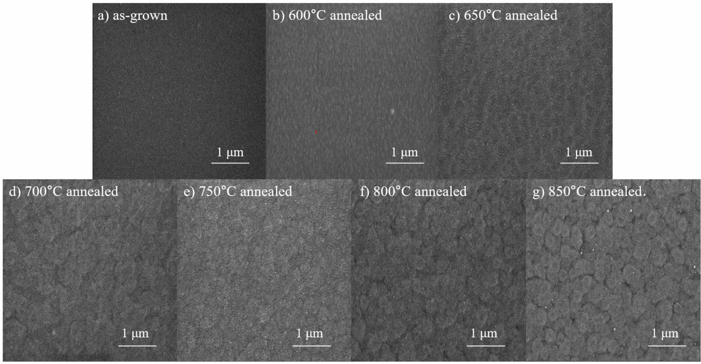
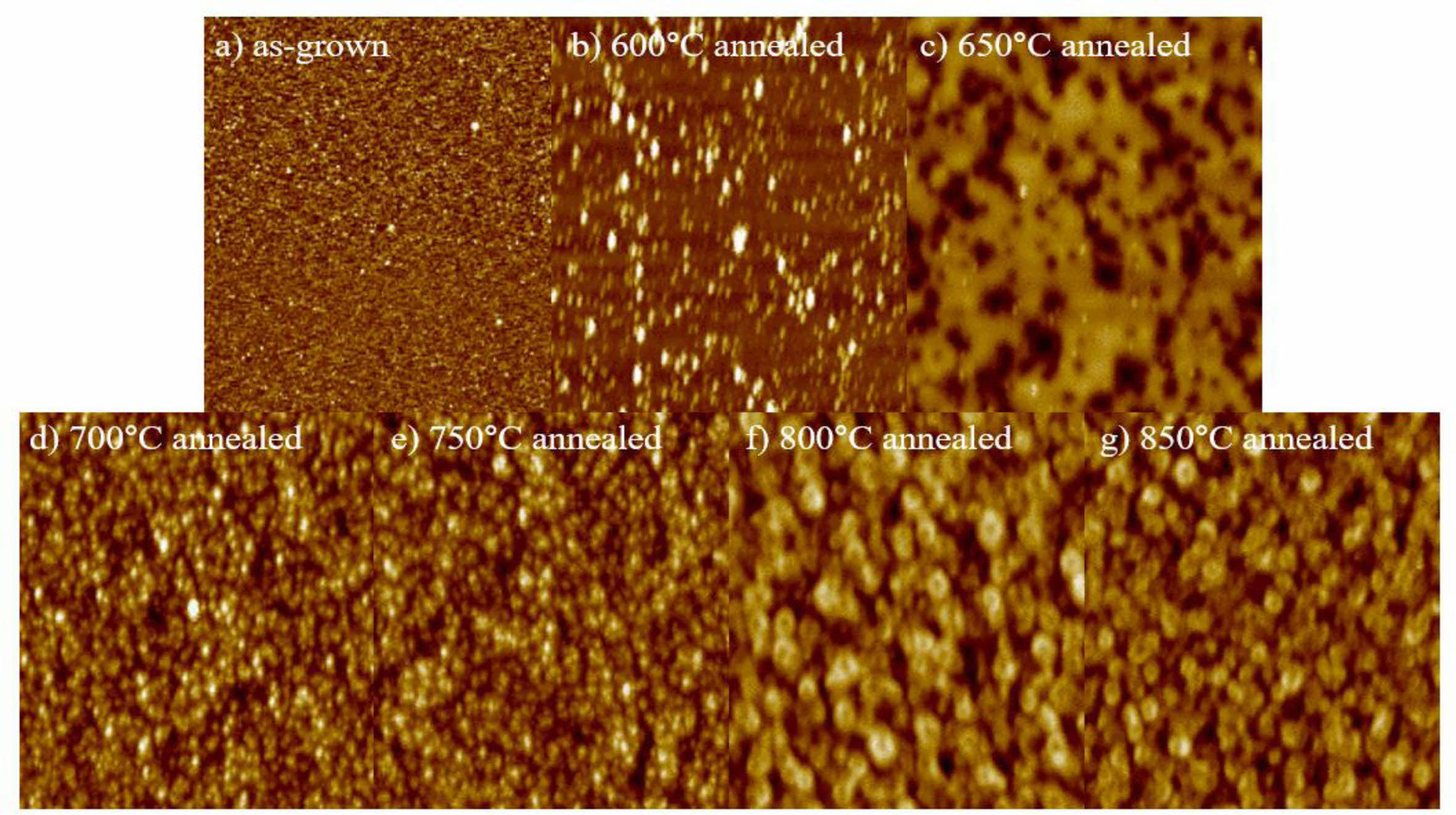
Fig. 1 shows 30k magnified SEM results of samples. From the SEM results, the as-grown sample exhibited a smooth surface. For the 600 °C sample, island formations were observed on the surface, indicating that the thin film transitioned to a Volmer-Weber growth mode due to insufficient thermal energy [11]. For the 650 °C sample, although it showed improvement compared to the 600 °C sample, it still failed to form a uniform thin film. This is attributed to insufficient growth conditions for the metastable ε-Ga₂O₃ phase, as supported by the XRD results [11, 12]. For the 700 °C and 750 °C annealed samples, sufficient thermal energy facilitated the formation of thin films through Frank-van der Merwe growth (2D growth) [11]. In contrast, for the 800 °C and 850 °C samples, the excessively high annealing temperatures resulted in the generation of crystal nuclei, resembling Stranski-Krastanov growth (3D growth) [11]. These observations were further corroborated by the AFM results. Fig. 2 shows AFM images scanned over an area of 5 μm × 5 μm of the annealed samples, with the RMS roughness values measured as follows: amorphous (0.788 nm), 600 °C (1.164 nm), 650 °C (2.156 nm), 700 °C (1.235 nm), 750 °C (1.281 nm), 800 °C (1.834 nm), and 850 °C (1.389 nm). The change in roughness indicates a distinct increase in roughness at 650 °C, where a complete 2D film was not formed, and at 800 °C, where the film began to transition to a 3D structure. The SEM image results clearly show that the roughness of the initially flat thin film changes due to the surface state variation caused by annealing. After the phase transition, the roughness decreased with further annealing at 700 °C-750 °C and 850 °C, suggesting surface restructuring due to the additional thermal energy [13].
Crystal Structure Analysis
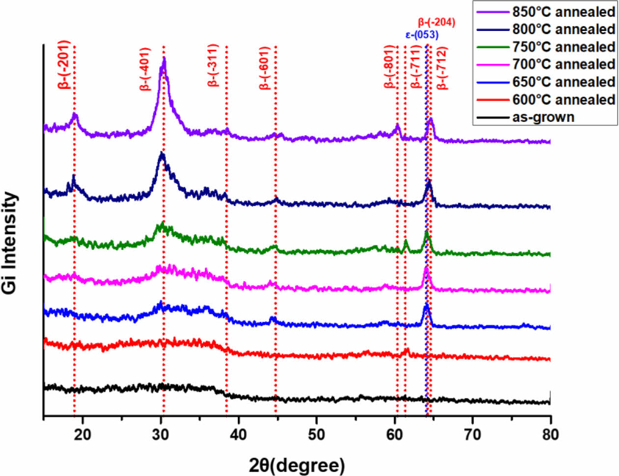
Fig. 3 shows the XRD results of as-grown and post annealed Ga₂O₃ thin films. The measurements were performed in a GI-mode with a fixed incident angle (θ) of 1°. For the as-grown and 600 °C annealed samples, an overall amorphous structure was observed, although a peak at 61.6° suggests the crystal structure was starting to change or on the verge of transformation. At 650 °C, a peak at 64.04° corresponding to the (3-30) ε-phase was observed [14]. For the 700 ℃ sample, it was challenging to determine whether it was at the boundary between ε-Ga₂O₃ and β-Ga₂O₃ phases. However, based on the absence of ε-Ga2O3 above 650 ℃, the sample was identified as β-Ga₂O₃ [15-17]. Distinct β peaks were observed at (64.08°) and (64.67°), corresponding to the (-204) and (-712) planes. For the 750 ℃ sample, the same β peaks as at 700 ℃ were identified, along with an additional peak at (61.27°) corresponding to the (-711) plane. For the 800 ℃ and 850 ℃ annealed samples, the influence of three-dimensional growth led to the observation of various additional β peaks at (18.91°), (30.46°), (38.39°), (44.74°), (60.52°), and (61.27°), corresponding to the (-201), (-401), (-311), (-601), (-801), and (-711) planes, respectively [JCPDS Card No.: 00-041-1103]. These results demonstrate that amorphous Ga₂O₃ transitions through the ε-phase to the β-phase with increasing annealing temperature.
XPS surface analysis.
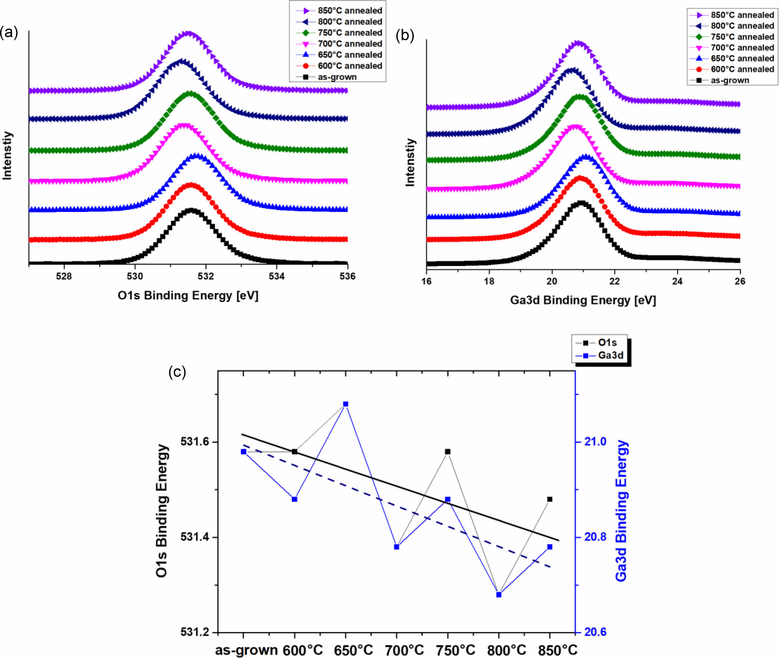
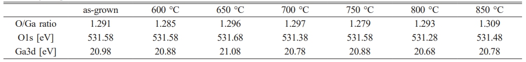
The binding energy for O1s in Ga₂O₃ typically consists of three components: OI (530.6 eV), corresponding to O²⁻ ions in the Ga₂O₃ lattice without oxygen vacancy, OII (531.2 eV), associated with oxygen-deficient regions, and OIII (532.1 eV), indicative of hydroxyl and carbonate species on the film surface [18]. The binding energy for Ga3d also consists of Ga metal (~18.6 eV), Ga₂O₃ (~20.6 eV) [19, 20]. The ideal ratio of O/Ga for Ga₂O₃ is 1.5, but the actual samples exhibited a lower O/Ga ratio (1.291 to 1.309). Fig. 4 shows (a) the binding energy changes of O1s, (b) the binding energy changes of Ga3d, and (c) the maximum binding energy changes of O1s and Ga3d. First, for the as-grown sample, the binding energies of O1s and Ga3d were 531.58 eV and 20.98 eV, respectively. This confirmed that Ga₂O₃ was well deposited, and at the same time, it was confirmed that the surface was amorphous Ga2O3-x due to the presence of numerous oxygen vacancies [18, 21-24]. The annealed samples also showed similar results since they were based on low-temperature growth. However, as the annealing temperature increased, the maximum binding energy values of O1s and Ga3d both decreased, which indicates that the surplus Ga ions, O ions, and electrons inside, which were not participating in the bonding, were recombined. The O/Ga ratio, O1s maximum binding energy, and Ga3d maximum binding energy for the as-grown amorphous Ga₂O₃ and annealed samples are summarized in Table 1.
Electrical characteristics analysis
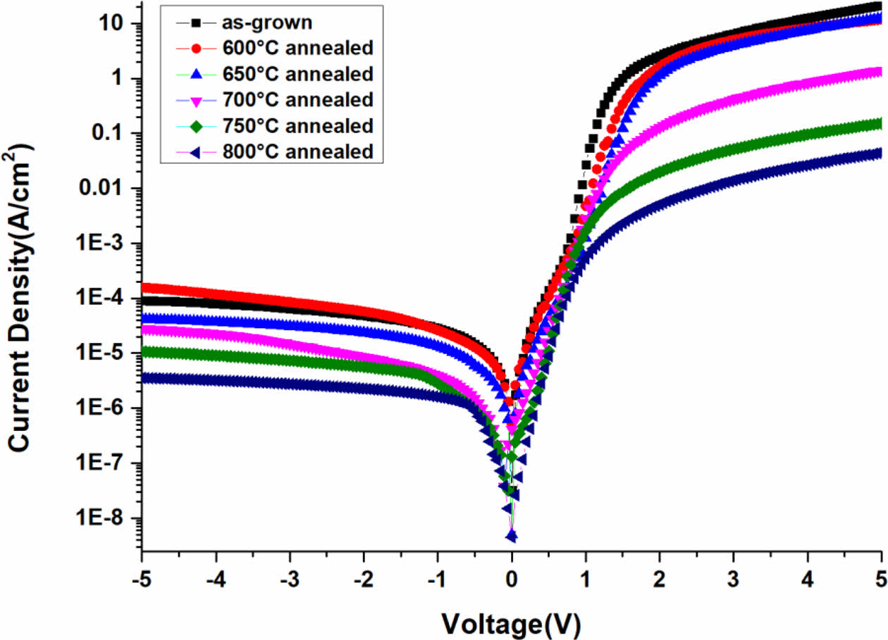
Fig. 5 shows the J-V results of the samples. As the annealing temperature increased, the current flow decreased, with a kink effect observed up to 650 °C. The forward J-V plot follows the thermionic emission mechanism described by the following equation:
where, J0: reverse saturation current density, V: applied voltage, q: electron charge, k: Boltzmann constant, η: ideality factor
By taking the natural logarithm of both sides, we get:
Additionally, J0 can be expressed as
A*: Richardson constant (= 41.1 A cm-2 K-2), ØB: Schottky barrier height
From eq. (3), ØB can be derived as:
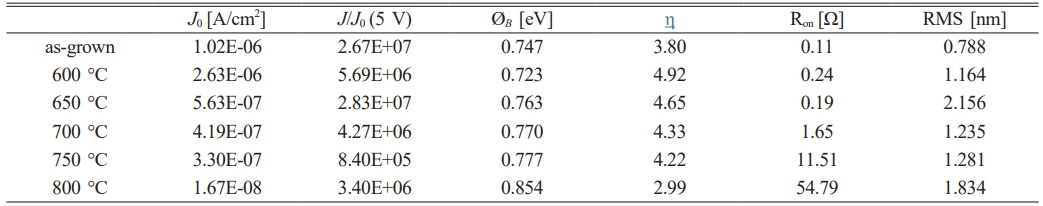
Using these equations, the ideality factor (η) [25], reverse saturation current density (J0), and Schottky barrier height (ØB) were calculated from the linear slope and intercept of the forward ln(J)-V plot [7, 25], and the on-state resistance (Ron) was determined from the slope of the forward J-V plot [7]. The results are summarized in Table 2.
As with the reduction in both forward and reverse J values due to phase transition by annealing, the J₀ value also decreased overall as the phase transitioned. The stoichiometric composition of Ga₂O₃ is crucial and significantly impacts its properties, particularly the bandgap, which is heavily influenced by thermal treatment and oxygen vacancies [26-29]. When there is an oxygen deficiency in the thin film, the disorder within the oxide causes the valence band maximum (VBM) to stretch, reducing the bandgap or increasing conductivity, indirectly decreasing the bandgap [26]. When thermal treatment is performed in such an oxygen-deficient state, internal excess gallium and oxygen ions recombine and oxidize, leading to a decrease in conductivity due to the reduced mobility, which ultimately results in the widening of the bandgap [27]. Furthermore, the changes in surface roughness and thin film properties due to phase transitions and the 2D/3D growth during thermal treatment also significantly affect the current flow. For instance, in samples with very rough surfaces and the 850 °C sample, the adhesion of the Ti/Au electrodes was significantly weakened, leading to poor electrode deposition. Even when the electrodes were deposited, inconsistent current results were observed due to factors like surface channels and voids. The Schottky barrier height (SBH,ØB) is determined by J₀ and the surface smoothness, and it was found to increase with phase transitions induced by higher annealing temperatures. For the amorphous as-grown sample and the 600 °C and 650 °C annealed samples, incomplete phase transition prevented the formation of a complete thin film, resulting in current characteristics similar to the amorphous as-grown state. Starting from 700 °C, where a complete beta-phase thin film was formed, both forward and reverse currents decreased. This was attributed to changes in the thin film's state, SBH changes, and the recombination of excess Ga and O ions, leading to a decrease in conductivity and an increase in Ron resistance, which gradually reduced current flow. The ideality factor (η) is highly influenced by interface states, surface defects, barrier height inhomogeneity, and high series resistance. As the annealing temperature increased, the current shape improved in a manner similar to the kink effect, and as the Ga-O bond ratio improved, the ideality factor also decreased.
|
Fig. 1 SEM images (30K magnified) of Ga2O3 thin films; as-grown amorphous (a) and post annealed at 600 °C (b), 650 °C (c), 700 °C (d), 750 °C (e), 800 °C (f) and 850 °C (g). |
|
Fig. 2 AFM images (scan 5 μm × 5 μm) of Ga2O3 thin films; as-grown amorphous (a) and post annealed at 600 °C (b), 650 °C (c), 700 °C (d), 750 °C (e), 800 °C (f) and 850 °C (g). |
|
Fig. 3 XRD patterns of as-grown Ga2O3 and post annealed Ga2O3 samples. |
|
Fig. 4 XPS binding energy spectra of (a) O1s, (b) Ga3d and (c) Changes in the maximum binding energy of O1s and Ga3d. |
|
Fig. 5 J-V characteristics of vertical SBD for as-grown Ga2O3 and post annealed samples. |
|
Table 1 Summarized values of the O/Ga ratio, maximum O1s binding energy, maximum Ga 3d binding energy depending on the annealing temperature. |
|
Table 2 Summarized values of the ideality factor (η), reverse saturation current density (J0), and Schottky barrier height (ØB) depend on the annealing temperature. |
Amorphous Ga₂O₃ was deposited on p-Si(111) substrates using MOCVD, and phase transitions induced by annealing were observed. From the SEM, AFM, and XRD results, it was confirmed that amorphous Ga₂O₃ transitioned to the ε-phase at 650 °C and to the β-phase at temperatures above 700 °C. However, at 600 °C and the ε-phase (650 °C), the conditions for obtaining a 2D phase transition thin film were not met, leading to an increase in roughness. At 800 °C and 850 °C, the thin film transitioned to 3D growth due to excessive energy, which also resulted in an increase in roughness. XPS results confirmed that Ga₂O₃ with a high oxygen vacancy was deposited, but oxygen vacancies decreased with annealing. In the current characteristics, the 600 °C and 650 °C annealed samples, which did not transition into a complete 2D phase thin film, showed current characteristics similar to the as-grown Ga₂O₃ due to significant influence from the amorphous phase. In contrast, the 700 °C, 750 °C, and 800 °C annealed samples, which transitioned to a complete β-phase, showed a decrease in both forward and reverse current due to changes in the surface state and the recombination of Ga and O, while the ideality factor improved.
This work was supported by a Korea Institute for Advancement of Technology (KIAT) grant funded by the Korea Government (MOTIE) (P0012451, The Competency Development Program for Industry Specialist). Also, this research was partially supported by the Korea Evaluation Institute of Industrial Technology (KEIT) grant funded by the Korea government (MOTIE) (RS-2022-00154720, Technology Innovation Program Development of next-generation power semiconductor based on Si-on-SiC structure).
- 1. S.J. Pearton, J. Yang, P.H. Cary IV, F. Ren, J. Kim, M.J. Tadjer, and M.A. Mastro, Appl. Phys. Rev. 5[1] (2018) 011301.
-

- 2. G. Joshi, Y.S. Chauhan, and A. Verma, J. Alloys Compd. 883 (2021) 160799.
-
- 3. H.J. Lee, S.M. Kang, T.I. Shin, J.W. Shur, and D.H. Yoon, J. Ceram. Process. Res. 9[2] (2008) 180-183.
-
- 4. N. Nepal, D.S. Katzer, B.P. Downey, V.D. Wheeler, L.O. Nyakiti, D.F. Storm, M.T. Hardy, J.A. Freitas, E.N. Jin, D. Vaca, L. Yates, S. Graham, S. Kumar, and D.J. Meyer, J. Vac. Sci. Technol. A. 38[6] (2020) 063406.
-
- 5. P. Sittimart, S. Ohmagari, T. Matsumae, H. Umezawa, and T. Yoshitake, AIP Adv. 11[10] (2021) 105114.
-
- 6. N.J. Ahn, J.B. An, J.Y. Lee, S.J. Mun, D.H. Lee, H.S. Ahn, K.H. Kim, and M. Yang, J. Ceram. Process. Res. 25[3] (2024) 439-445.
-
- 7. M.K. Yadav, A. Mondal, S.K. Sharma, and A. Bag, J. Vac. Sci. Technol. A 39[3] (2021) 033203.
-
- 8. H.W. Kim, N.H. Kim, and C. Lee, Adv. Appl. Ceram. 103[4] (2004) 187-189.
-
- 9. H.Y. Playford, A.C. Hannon, E.R. Barney, and R.I. Walton, Chem. Eur. J. 19[8] (2013) 2803-2813.
-
- 10. R. Roy, V.G. Hill, and E.F. Osborn, J. Am. Chem. Soc. 74[3] (1952) 719-722.
-
- 11. A.C. Levi and M. Kotrla, J. Phys.: Condens. Matter 9[2] (1997) 299-344.
-
- 12. Y. Yao, S. Okur, L.A.M. Lyle, G.S. Tompa, T. Salagaj, N. Sbrockey, R.F. Davis, and L.M. Porter, Mater. Res. Lett. 6[5] (2018) 268-275.
-
- 13. F. Shi, J. Han, Y. Xing, J. Li, L. Zhang, T. He, T. Li, X. Deng, X. Zhang, and B. Zhang, Mater. Lett. 237 (2019) 105-108.
-
- 14. S. Yoshioka, H. Hayashi, A. Kuwabara, F. Oba, K. Matsunaga, and I. Tanaka, J. Phys.: Condens.Matter 19[34] (2007) 346211.
-
- 15. D. Hu, S. Zhuang, Z. Ma, X. Dong, G. Du, B. Zhang, Y. Zhang, and J. Yin, J. Mater. Sci.: Mater. Electron. 28 (2017) 10997-11011.
-
- 16. T. Kusaba, P. Sittimart, Y. Katamune, T. Kageura, H. Naragino, S. Ohmagari, S.M. Valappil, S. Nagano, A. Zkria, and T. Yoshital, Appl. Phys. Express 16[10] (2023) 105503.
-
- 17. F. Boschi, M. Bosi, T. Berzina, E. Buffagni, C. Ferrari, and R. Fornari, J. Cryst. Growth 443 (2016) 25-30.
-
- 18. L.-X. Qian, Z.-H. Wu, Y.-Y. Zhang, P.T. Lai, X.-Z. Liu, and Y.-R. Li, ACS Photonics 4[9] (2017) 2203-2211.
-
- 19. S. Manandhar, A.K. Battu, S. Tan, R. Panat, V. Shutthanandan, and C.V. Ramana, J. Mater. Sci. 54[17] (2019) 11526-11537.
-
- 20. S.C. Ghosh, M. C. Biesinger, R.R. LaPierre, and P. Kruse, J. Appl. Phys. 101[11] (2007) 114322.
-
- 21. S. Pal, R. Mahapatra, S.K. Ray, B.R. Chakraborty, S.M. Shivaprasad, S.K. Lahiri, and D.N. Bose, Thin Solid Films 425[1-2] (2003) 20-23.
-
- 22. T.A. Chowdhury, Engineering 15[8] (2023) 459-466.
-
- 23. A. Navarro-Quezada, Z. Galazka, S. Alamé, D. Skuridina, P. Vogt, and N. Esser, Appl. Surf. Sci. 349 (2015) 368-373.
-
- 24. J.H. Yu, T.S. Jeong, C.J. Youn, T.S. Kim, and K.J. Hong, J. Ceram. Process, Res. 17[5] (2016) 419-425.
-
- 25. H. Zhou, Q. Yan, J. Zhang, Y. Lv, Z. Liu, and Y. Zhang IEEE Electron Device Lett. 40[11] (2019) 1788-1791.
-
- 26. M.D. Heinemann, J. Berry, G. Teeter, T. Unold, and D. Ginley, Appl. Phys. Lett. 108[2] (2016) 022107.
-
- 27. L. Nagarajan, R.A.D. Souza, D. Samuelis, I. Valov, A. Börger, J. Janek, K.-D. Becker, P.C. Schmidt, and M. Martin, Nat. Mater. 7[5] (2008) 391-398.
-
- 28. A. Petitmangin, C. Hébert, J. Perrière, B. Gallas, L. Binet, P. Barboux, and P. Vermaut, J. Appl. Phys. 109[1] (2011) 013711.
-
- 29. J. Wu, W. Mi, Z. Yang, Y. Chen, P. Li, J. Zhao, K. Zhang, X. Zhang, and C. Luan, Vaccum 167 (2019) 6-9.
-
 This Article
-
2025; 26(2): 197-202
Published on Apr 30, 2025
- 10.36410/jcpr.2025.26.2.197
- Received on Oct 18, 2024
- Revised on Dec 17, 2024
- Accepted on Dec 20, 2024
Services
Shared
Correspondence to
- Min Yang
-
Department of Nano Semiconductor Engineering, Korea Maritime and Ocean University, Busan 49112, Korea
Tel : +82-10-3648-2551 Fax: +82-51-404-3986 - E-mail: myang@kmou.ac.kr
Clean-Energy Research Institute(CRI), Hanyang University, 222, Wangsimni-ro, Seongdong-gu, Seoul, 04763, Korea
E-mail: jcpr@hanyang.ac.kr