


- Study of effect of high-energy grinding and niobium-doping on the semiconducting properties of the CaTiSiO5 compound
Pablo C. Carbo-Velab,*, José M. Almanza-Roblesa, Dora A. Cortés-Hernándeza, José C. Escobedo-Bocardoa, José A. Rodríguez-Garcíab and Wilian J. Pech-Rodríguezb
aCentro de Investigación y de Estudios Avanzados del Instituto Politécnico Nacional Unidad Saltillo, Ave. Industria Metalúrgica No. 1062, Parque Industrial Saltillo-Ramos Arizpe, C.P. 25900, Ramos Arizpe, Coahuila, México
bUniversidad Politécnica de Victoria, Av. Nuevas Tecnologías No. 5902, Parque Científico y Tecnológico de Tamaulipas, C.P. 87138, Cd. Victoria, Tamaulipas, MéxicoThis article is an open access article distributed under the terms of the Creative Commons Attribution Non-Commercial License (http://creativecommons.org/licenses/by-nc/4.0) which permits unrestricted non-commercial use, distribution, and reproduction in any medium, provided the original work is properly cited.
Titanite (CaTiSiO5) was prepared from a mixture of CaCO3, TiO2 and SiO2 with and without high-energy mechanical activation. Niobium-doped titanite samples were prepared without mechanical activation from a mixture of CaCO3, TiO2, SiO2 and Nb2O5 according to CaTi1-xNbxSiO5, where x = 0.0, 0.05, 0.1 and 0.15. All samples were heat treated at 1250°C for 4 h. Then, samples were characterized by X-ray diffraction (XRD) and UV-vis spectroscopy and selected samples were evaluated by cyclic voltammetry. Titanite was obtained as a single phase in samples with mechanical activation while the no activated sample showed the presence of second phases. The band gap values are within the range of semiconductor materials (3.34 and 3.47 eV). The current densities under off and on conditions were 1.06 and 1.65 mAcm-2, respectively. These values are related to the oxygen evolution reaction. The more appropriated results were obtained for the titanite obtained with mechanical activation. On the other hand, according to X-ray diffraction results, the maximum amount of Nb-doped titanite obtained after heat treatment was 95.1 wt.%. The band gap was reduced, from 3.48 to 3.36 eV, as Nb concentration was increased. Nonetheless, all titanite-based compounds are semiconductor materials suitable to be used as photocatalytic materials.
Keywords: High-energy ball milling, Photo-electrochemical properties, Calcium titanium silicate, Doping process, Powders.
Titanite is a mineral classified within the nesosilicates. It has monoclinic symmetry and crystallizes in the space group A 2/α and P 21/α. Titanite (CaTiSiO5) is found naturally in igneous and mesomorphic rocks [1]. As it is one of the sources of titanium dioxide its name “titanite” is due to its high content of titania or titanium dioxide. Titanite allows substitutions within its structure such as Nb, Al, Fe, Cr and U. In the last decades this compound has received interest by mineralogists and researchers [2-9].
Speer and Gibbs [10] reported that the microstructural parameters of titanite allow it to host different ions into its structure. Their applications are diverse and it has been used for the immobilization of radioactive waste [11, 12], pigments [13, 14], orthopedic and dental implants [15, 16] and antibacterial applications [17, 18].
The methods used for preparation of titanite are sol-gel [16, 19], coprecipitation [19], combustion [19], spray pyrolysis [20] and solid-state reaction [17, 18]. Nevertheless, obtaining pure titanite is difficult to achieve. The solid-state-reaction synthesis has been carried out by mechanical activation in order to obtain a higher percentage of titanite [21-23]. The mechanical activation route is simple and allows to obtain more homogeneous materials. In addition, this method can be implemented for industrial processing [24, 35].
Niobium is a common constituent of mineral titanite, VIIAVIBSiO5, where A = Ca, Na, Sr, Mn, rare earth elements, and B = Ti, Sn, Sb, Al, Fe, Zr, Ta, Nb. Niobium-doped titanite has been prepared by solid state reaction method as reported in the literature [2], where Ti is partially substituted by either Nb or Al. All Nb-doped varieties of titanite adopt a space group A2/a, in which all cations in positions A and B are located at random sites. Both Nb-doped titanite and pure CaTiSiO5 consist of distorted polyhedra. The synthetic Nb-doped titanite compositions may be suitable for the encapsulation of radioactive waste [2].
Nb-doped TiO2 [36] has been used for coating the anodes in photoelectrochemical devices as lithium-ion batteries. In this process, the use of preliminary mechanical activation plays an important role for successfully obtaining the Nb-doped TiO2 by solid-state synthesis. The mechanical activation decreased the temperature and calcination time, in comparison to those of the conventional ceramic synthesis. The formation and homogeneous distribution of submicron TiNb2O7 particles enhances the electrochemical performance improving conductivity [36]. The theoretical electrochemical capacity of TiNb2O7 is comparable with that of graphite.
In this study, the optical and photocatalytic properties of materials based on titanite obtained with and without mechanical activation were evaluated. On the other hand, the effect of Nb-doping of titanite, were evaluated in the same properties.
Sample preparation
Nb-doped titanite samples without mechanical activation were prepared according to the following formulation: CaTi1-xNbxSiO5, where x = 0.0, 0.05, 0.1 and 0.15. Titanite samples were obtained from a powder mixture of CaCO3 (Barmex, 99%), TiO2 (Merck, 99%), Nb2O5 (Inframat, 99%) and SiO2 (Materias Primas Minerales de San José, 99%). The sample mixture without mechanical activation was homogenized in a jar with alumina balls using acetone as dispersing medium for 3 h in spinning rods. Powders were dried at 80°C for 24 h. Pellets of 10 mm in diameter and 5 mm in height were conformed by uniaxial pressing at 63 MPa. Pellets were heat treated at 1250°C for 4 h at a heating and cooling rate of 5°Cmin-1.
The mechanical activation process of powders was carried out in air at room temperature in an attrition mill operated at 1590 rpm. The mill was charged with 30 g of powder (15.31 g of CaCO3, 12.22 g of TiO2 and 9.19 g of SiO2) for each milling time using 100 ml of ethanol as dispersant, occupying in total approximately two-thirds of the volume of the mill container. Powder mixtures were homogenized for 6, 8 and 10 h using Al2O3 balls with a diameter of 1mm as milling media. A ball/load mass ratio of 5/1 was used. After milling, mixtures were dried at 80°C for 24 h. Pellets of 10 mm in diameter and 5 mm in height were conformed by uniaxial pressing at 63 MPa. Pellets were heat treated at 1250°C in air (Thermoscientific Lindberg Blue M) for 4 h at a heating and cooling rate of 5°Cmin-1.
Characterization of samples
After sintering, samples were analyzed by X-ray diffraction (XRD, Philips®, Mod. X´Pert PW3040) using a current of 30 mA and a voltage of 40 kV in a 2θ range from 10° to 80° with a scanning step size of 0.02° and mean Cu Kα wavelength: 1.5418 × 10⁻¹⁰ m. The XPowder 12 software (Ver. 2014.04.36) was used for quantification on full profile of the diffractograms by non-linear least squares regression. The UV-vis absorption spectra of the sintered samples were obtained by diffuse reflectance studies using a PerkinElmer® spectrophotometer Lambda 365 model with integration sphere using BaSO4 as a white standard for 100% of reflectance. Current density was determined by the cyclic voltammetry technique using a Gill AC potentiostat-galvanostat (ACM Instruments®) and a solar simulator (ABET Technologies® model 11002), under on illumination conditions (100 mWcm-2, AM 1.5G).
Electrochemical experiments
Cyclic voltammetry (CV) and linear sweep voltammetry (LSV) techniques were performed with a standard three-electrode system to identify the changes in the photoelectrochemical potential of the oxidation and reduction processes of the catalyst used (sample). A glassy carbon electrode was used as the working electrode, graphite wire electrode and Ag/AgCl acted as the auxiliar and reference electrode, respectively. The electrochemical active area of the working electrode (Ø = 5 mm) was estimated using CV and LSV techniques using a 0.5 molL-1 H2SO4 aqueous solution as a medium. The CV was activated at a scan rate of 50 mVs-1 and then 3 cycles at a scan rate 20 mVs-1. On the other hand, LSV was recorded at a scan rate of 5 mVs-1. The CV potential scan ranges from 0 to 1000 mV and LSV from 500 to 1700 mV.
Samples with mechanical activation
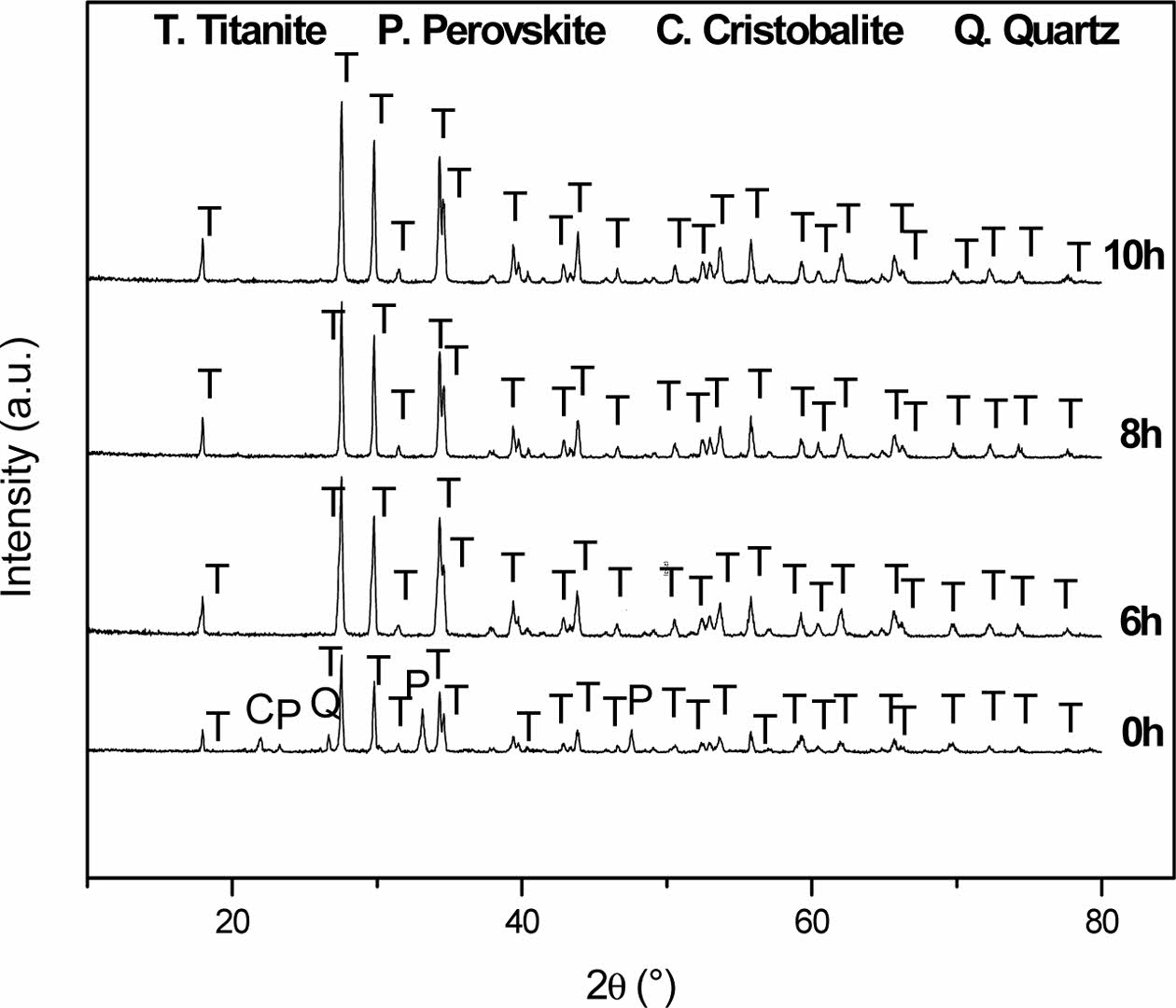
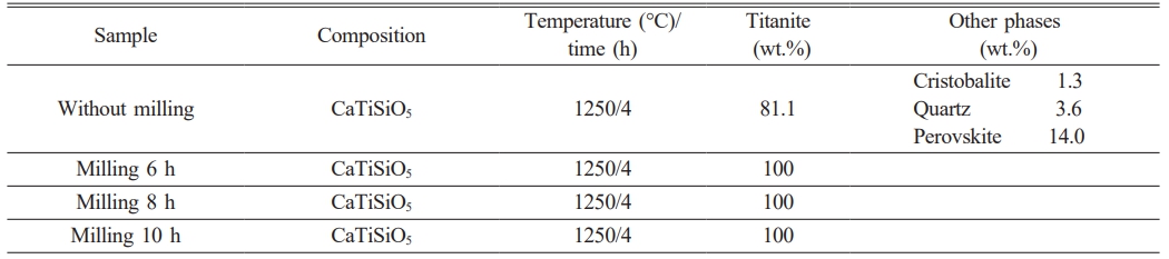
Fig. 1 shows the XRD patterns of the titanite-based ceramics with the following milling times: 0, 6, 8 and 10 h. The main phases detected were titanite (JCPDS: 87-0256; monoclinic; CaTi(SiO4)O), cristobalite (JCPDS: 77-1317; tetragonal; SiO2), perovskite (JCPDS: 88-0790; orthorhombic; Ca(TiO3)) and quartz (JCPDS: 33-1161; hexagonal; SiO2). The titanite, perovskite, cristobalite and quartz phases were labeled as T, P, C and Q, respectively.
Table 1 shows the semi-quantitative analysis of the samples before and after high-energy milling. As observed, high energy milling promoted the formation of a single phase (titanite).
It is known that mechanical activation leads to materials with smaller particle size, larger surface area, higher number of defects and a high accumulated energy, which favors chemical reactions, promoting the formation of the desired compound at lower temperature. According to these results, 80% of titanite is obtained with no mechanical milling while 100% of titanite is obtained when powder mixtures are mechanically activated. The results of this process are comparable to those reported in the literature [21, 22].
The mean particle size of titanite-based ceramics with the milling times: 6, 8 and 10 h, obtained before any calcinations were 15.976, 37.246 and 12.594 µm, respectively, which were obtained by laser diffraction technique (Particle Size Analyzer (HORIBA, LA-950)). The particle size of sample milled at 8 h was higher than that of the sample milled for 10 h due to an agglomeration of particles during milling processes.
The band gap values of all the samples were obtained using the Tauc method [25]. Equations (1) and (2) were used to calculate band gap (Eg).

where α is the absorption coefficient, A is the absorption constant, hν is the photon energy and n can take different values depending on the type of the electron transition and is equal to 1/2 or 2 for the direct and indirect transition band gaps, respectively.
Band gap values were calculated using equation (2), where ν = C/λ.

where h = Planck constant (6.626 × 10⁻³⁴ J.s), C = speed of light (3.0 × 10⁸ ms-1), λ = cut off wavelength (m) and, finally, the conversion considering that 1 eV = 1.609 × 10⁻¹⁹ J.
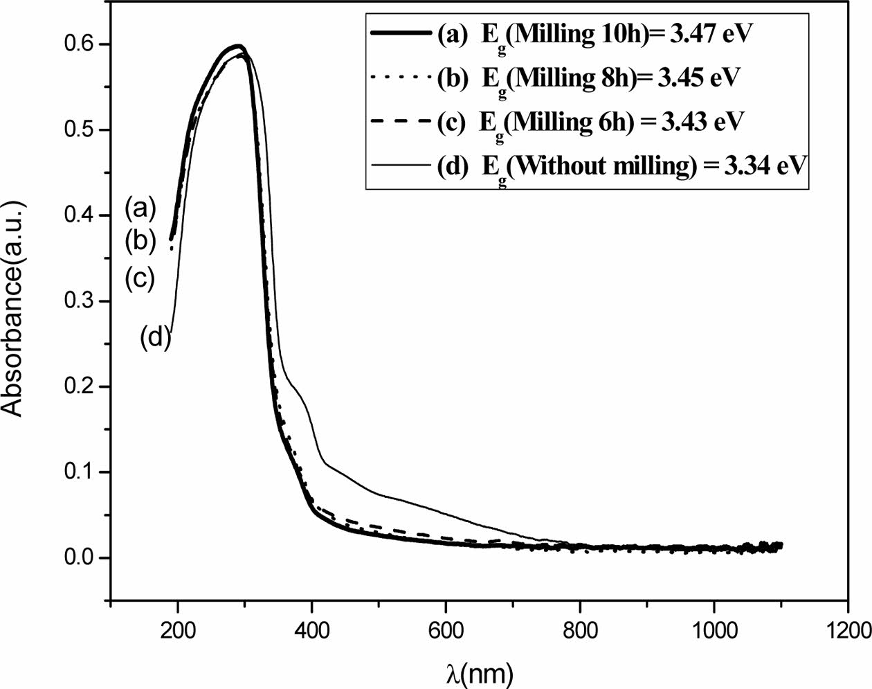
When α = 0, Eg = hν, which was calculated from the UV-vis spectra by extrapolating a straight line from the absorption curve to the abscissa axis. The band gap value obtained for the sample without milling was 3.34 eV, while for 6, 8 and 10 h samples the band gap values were 3.43, 3.45 and 3.47, respectively. Band gap values were also calculated using the Kubelka-Munk model [26], where only diffuse light is considered. These values were similar to those obtained by the Tauc method and indicate that these titanite materials are appropriate semiconductors.
Fig. 2 shows the absorption spectra of CaTiSiO5 based ceramic materials obtained before and after milling.
As it can be observed in Fig. 2, the band gap of these titanite-based materials are within the range of that corresponding (2.75-3.6 eV) to the semiconductor materials [17, 27]. Furthermore, according to the literature, the threshold for direct optical transition from the valence band to the conduction band for titanite has been reported, the electron requires less energy to make a transition between bands and it is more efficient in its optical emission, and this is true in titanite-based materials [35]. Nevertheless, according to the results shown in the Fig. 2, band gap increases as the milling time was increased. This may be due to the reduction in the crystallite size [30-33].
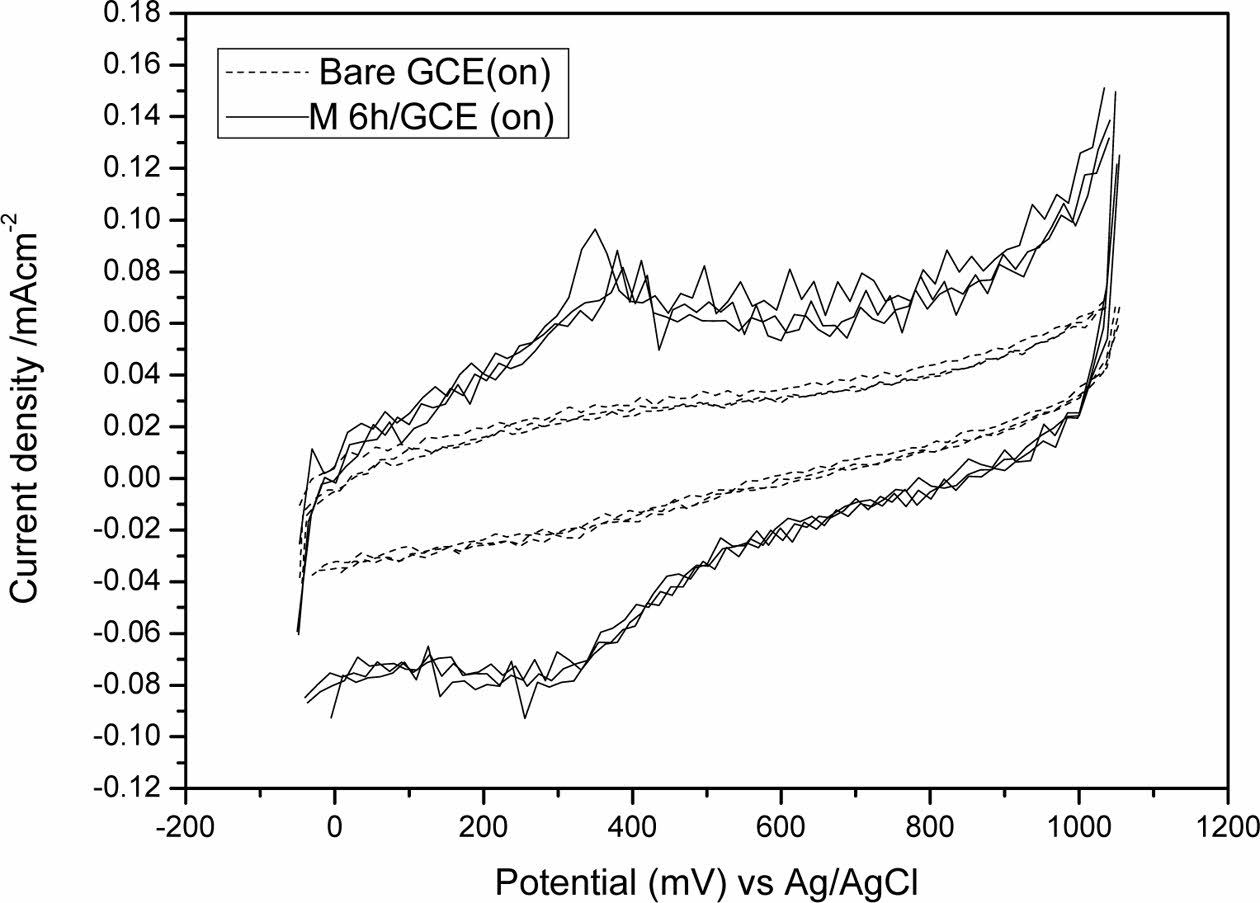
Fig. 3 shows the cyclic voltammograms, testing was performed using glassy carbon electrode only (Bare GCE) without and with the based ceramic material obtained using mechanical activation (after 6 h milling (Milling 6 h/GCE)), both under on illumination conditions. The reason why the choice of Milling 6 h sample is due to the less required energy for the trials.
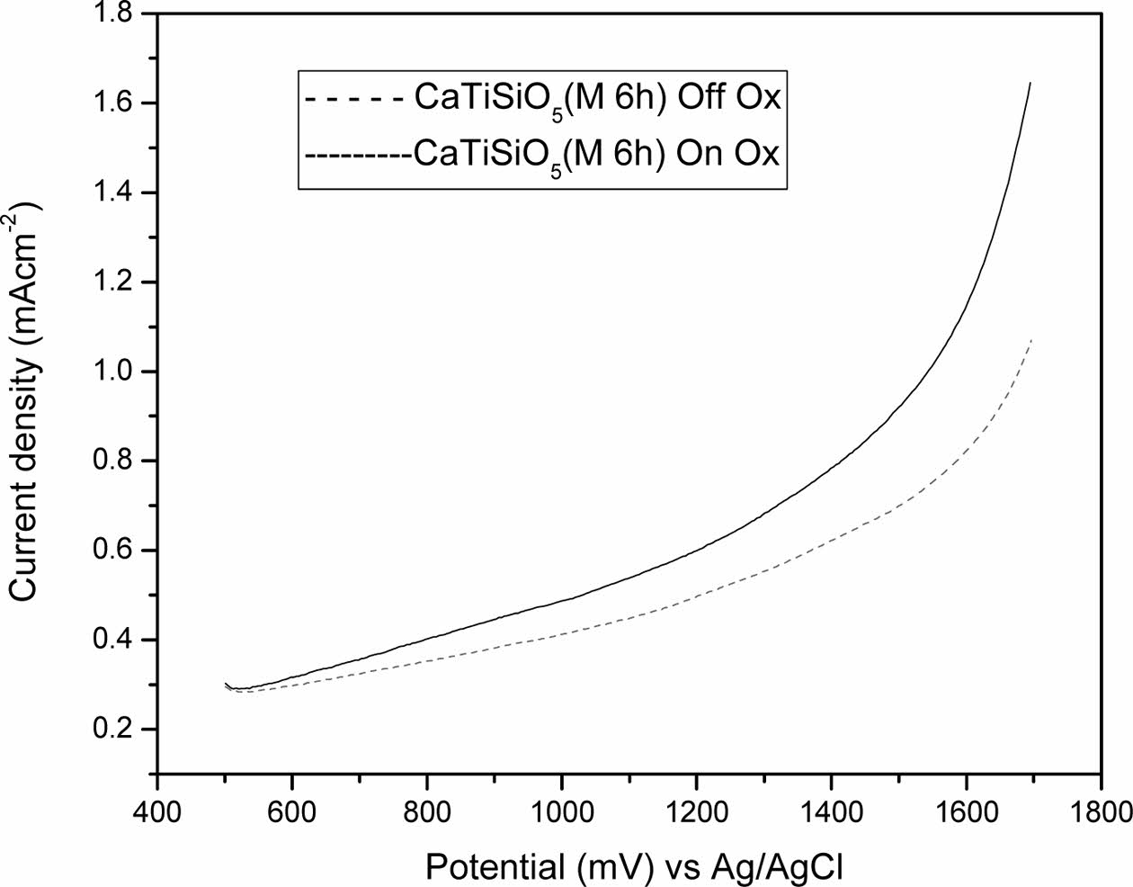
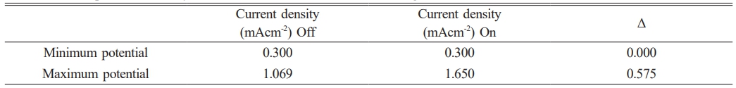
LSV of titanite, scanned at anodic potentials between 500 and 1700 mV in 0.5 M H2SO4 aqueous solution, are shown in Fig. 4. The values were obtained under off-on conditions in order to determine the photo-electrocatalytic activity. Under dark conditions (dotted lines), electrodes exhibited a very small current, while under illumination conditions, the photocurrent increased to the range of 1.069 to 1.65 mAcm-2, with potentials higher than 1400 mVAg/AgCl. The current shown in Fig. 4 and Table 2 is related to the oxygen evolution reaction, similar values (0-2 mAcm-2) were reported in the literature for semiconductor ceramics [28, 29, 34].
Table 2 shows current density values (VC technique under off-on conditions) of titanite obtained at a milling time of 6 h.
Table 2 shows a minimum potential of 0.300 mAcm-2 and a maximum potential of 1.069 mAcm-2 under off illumination condition, while at on illumination a minimum potential of 0.300 mAcm-2 and maximum potential of 1.650 mAcm-2 are observed. Results showed in Fig. 4 and Table 2 suggest that the current density, associated to the oxygen evolution, increases by 50% under illumination conditions, which indicates that these materials have appropriated properties in photoelectrochemical applications.
Photoelectrochemical behavior of the mechanical activated titanite electrode was analyzed using the data obtained by the voltametric experiments and it was demonstrated that the photocurrent signal is significantly enhanced under on illumination condition [38]. This effect was attributed to the high tendency to scavenge the photogenerated holes during light illumination, which may effectively increase the photoconversion efficiency of hydrogen generation by lowering the potential and increasing the photocurrent. Based on these results, the working electrode (Milling 6 h/GCE) can be used as a photoelectrochemical sensor [28].
Its important to stablish a relationship between changes occurred on the ball-milling process and doping of titanite-based materials, and one of these relations is about determine their optical and photoelectrochemical properties but separately and then, compare such changes. The next section describes the niobium-doping process.
Samples with niobium-doping process
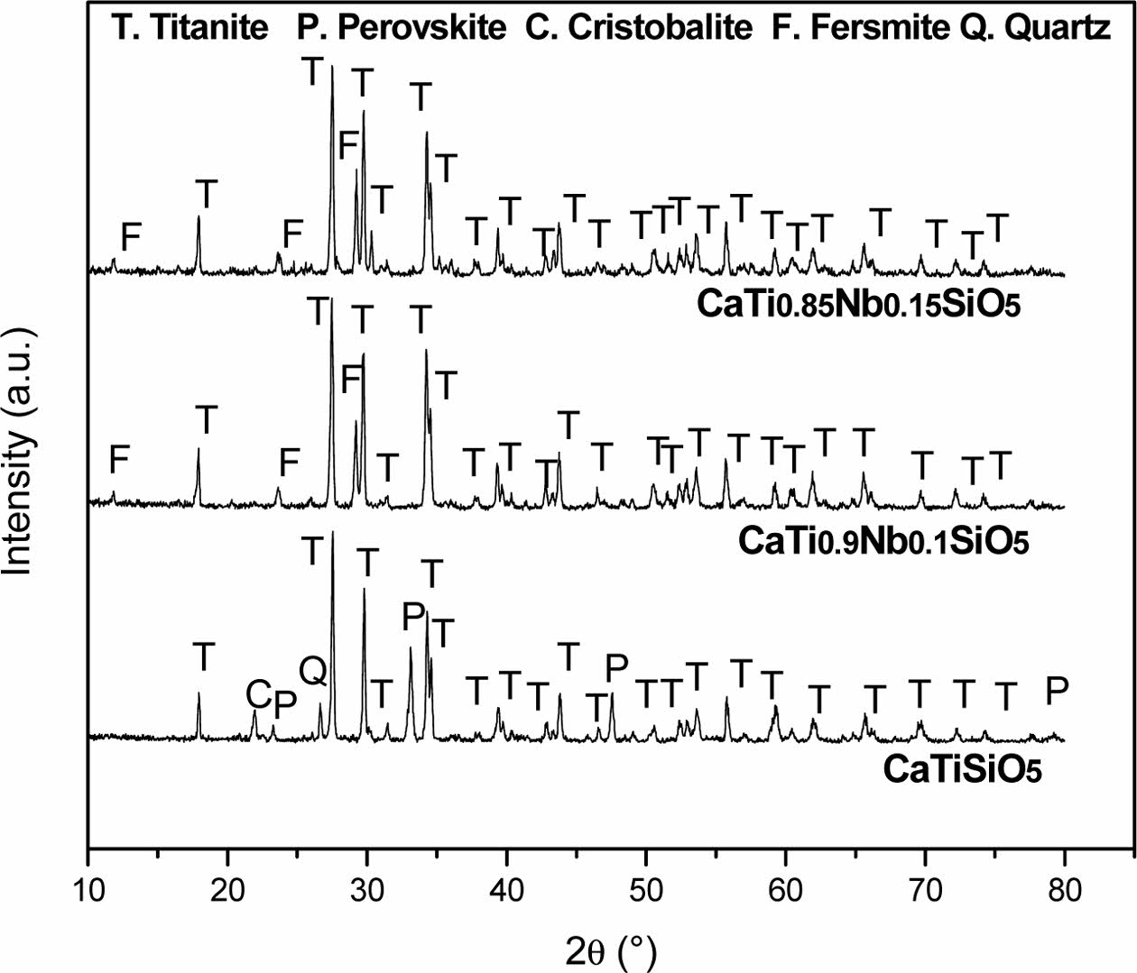
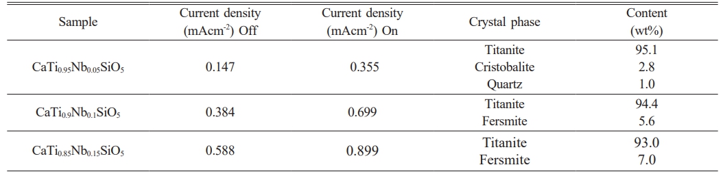
Fig. 5 shows the XRD patterns of the Nb-doped titanite-based ceramics. The main phases detected were titanite (JCPDS: 87-0256; monoclinic; CaTi(SiO4)O); cristobalite (JCPDS:77-1317; tetragonal; SiO2), perovskite (JCPDS: 88-0790; orthorhombic; Ca(TiO3)) and fersmite (JCPDS: 71-2406; orthorhombic; CaNb2O6) and quartz (JCPDS: 33-1161; hexagonal; SiO2). The titanite, perovskite, cristobalite, fersmite and quartz phases were labeled as T, P, C, F and Q, respectively.
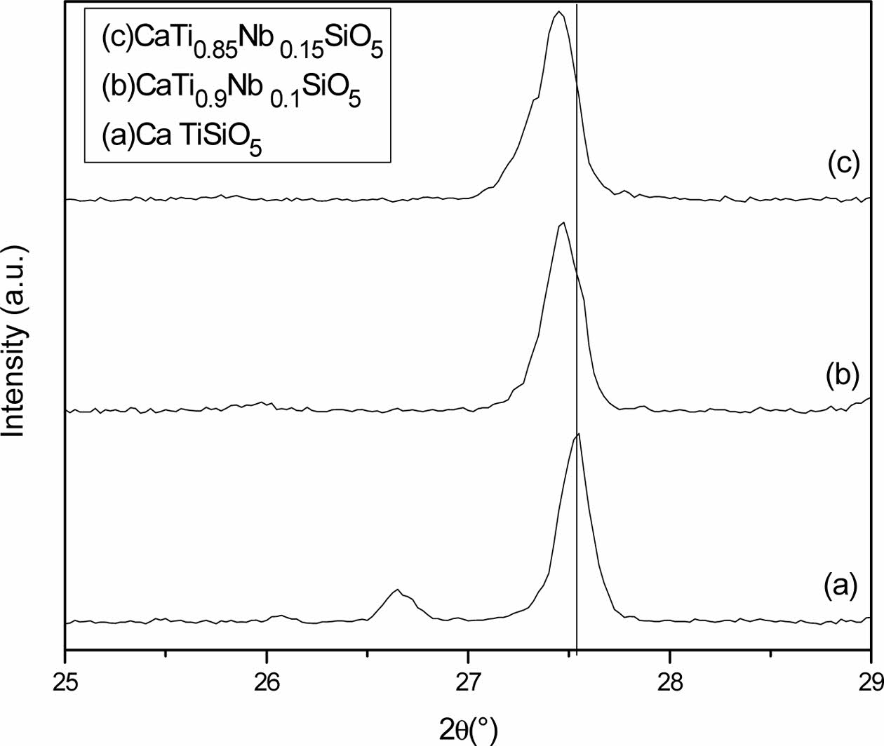
The titanite content in the non-doped sample, determined by X-ray diffraction, was only 81.1%. As the Nb concentration is increased, the quantity of the formed titanite was also increased. On the other hand, Fig. 6 shows that the peaks corresponding to titanite are shifted towards lower 2θ angle due to the Nb-doping and the difference in crystal structure of different phases affect position of diffraction peaks. Hence two substances having different crystal structures will produce different sets of XRD scans. Table 3 shows the semi-quantitative analysis of phases obtained by the X-Powder software using the corresponding XRD spectra. This table shows also the current density values of titanite-based compounds at different Nb concentration obtained by the CV technique under off-on conditions.
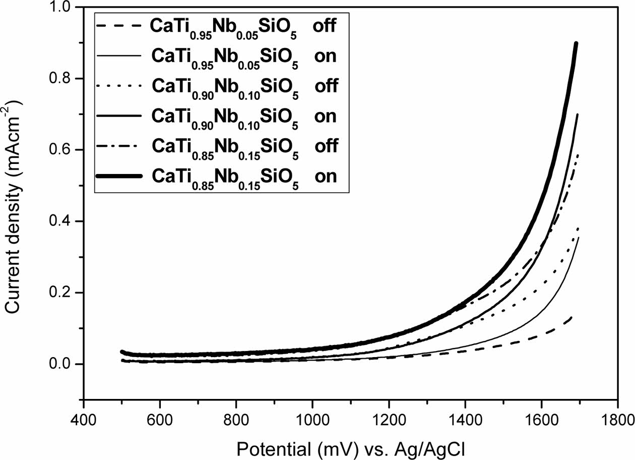
LSV of Nb-doped titanite scanned at anodic potentials between 500 and 1700 mV in 0.5M H2SO4 aqueous solution, are shown in Fig. 7. The values were obtained under off-on conditions in order to determine photo-electrocatalytic activity. Under the dark (dotted lines), the electrodes exhibited a very small current, and under on illumination, the photocurrent increased up to values within the range of 0.355 and 0.899 mAcm-2 as the Nb concentration was increased, with potentials higher than 1400 mVAg/AgCl. Results showed in Fig. 7 and Table 3 suggest that the current density, associated to the oxygen evolution, increases by 50% under illumination conditions, which indicates that these materials have appropriated properties in photoelectrochemical applications.
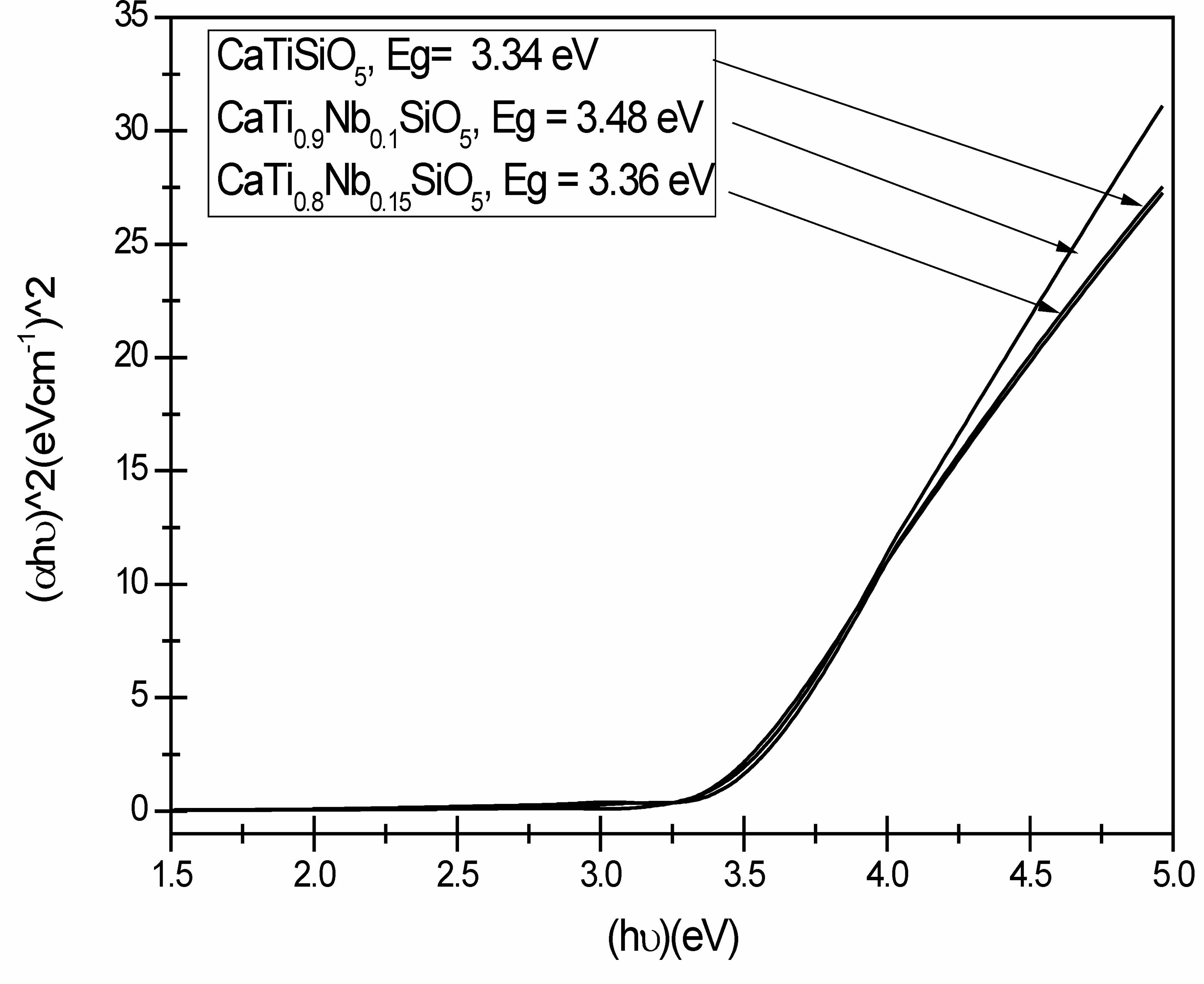
Fig. 8 shows the UV-vis spectra of Nb-doped titanite samples and their band gap values obtained using the Tauc method.
As it can be observed in Fig. 8, the band gap of these Nb-doped titanite-based materials are within the range of that corresponding (2.75-3.6 eV) to the semiconductor materials [17, 27]. Furthermore, according to the literature, the threshold for direct optical transition from the valence band to the conduction band for titanite has been reported, and it was stated that the electron requires less energy to make a transition between bands and it is more efficient in its optical emission [35]. According to the results shown in the Fig. 8, band gap decreases as the Nb-doping was increased. This may be due to presence of the substituting element, in this case Nb, which is partially occupying Ti sites into the crystallographic structure, this may increase the quantity of defects. Band gap of semiconductor changes when foreign impurities are added. Increase or decrease in band gap will depend which element in the semiconductor is replaced by which element. The changes in the properties of the titanite-based materials such as structural disorder and energy band-gap were correlated with the incorporation of Nb in their structure. Improvement of the optical and photoelectrochemical properties was achieved by a high thermal treatment and its potential applications, for example, as niobium oxide nanostructures on substrates [37, 39].
|
Fig. 1 XRD patterns of CaTiSiO5 materials at milling times of 0, 6, 8 and 10 h. |
|
Fig. 2 Diffuse reflectance UV-vis spectra of (a) Milling 10 h, (b) Milling 8 h, (c) M 6 h and (d) Without milling. |
|
Fig. 3 Cyclic voltammograms obtained with only glassy carbon electrode (Bare GCE) vs. Milling 6 h/GCE under on illumination condition. |
|
Fig. 4 Linear sweep voltammograms (LSV) of milling 6 h scanned at anodic potentials between 500 and 1700 mV, scan rate of 5 mVs-1. |
|
Fig. 5 XRD patterns of CaTiSiO5 based materials doped with different quantities of Nb. |
|
Fig. 6 XRD patterns of Nb-doped CaTiSiO5 based materials (25-29° 2 theta region). |
|
Fig. 7 Linear sweep voltammetry of Nb-doped CaTiSiO5 at high anodic potential in 0.5M H2SO4, scan rate = 5 mVs-1. |
|
Fig. 8 UV-visible spectra of the Nb-doped titanite samples obtained using the Tauc method. |
|
Table 1 Semi-quantitative analysis of the titanite-based compounds at different milling times. |
|
Table 3 Semiquantitative analysis and electrochemical values of titanite-based compounds doped with different quantities of Nb. |
Pure titanite was obtained processing the precursor powders by high-energy milling attrition. When powders were not milled, samples showed second phases such as cristobalite, perovskite and quartz, apart from titanite. The band gap increased from 3.43 to 3.47 eV as the milling time was increased due to the reduction of crystallite size, while samples without mechanical activation showed a band gap of 3.34 eV. Results of the electrochemical analysis showed that the current density, associated to the oxygen evolution, increases by 50% under illumination conditions.
Nb-doped titanite (CaTiSiO5) was obtained without mechanical activation from a mixture of TiO2, SiO2, CaCO3 and Nb2O5. The XRD reflections corresponding to titanite showed a displacement to lower values in 2θ as the Nb amount was increased, which indicates the incorporation of Nb into the titanite crystalline structure. The band gap decreases as the Nb amount was increased. Furthermore, current density increased in about 50% under illumination condition as the Nb content was increased. According to the results obtained, these materials are potential candidates for photo-electrocatalytic applications.
The powders obtained in both no milled and milled were analyzed by different techniques. At the same time niobium-doping process showed similarities about optical and photoelectrochemical properties between mechanical activation and doping processes.
Financial support provided by the National Council of Science and Technology (CONACyT) is gratefully acknowledged.
The authors declare no conflict of interest.
This research received no external funding.
- 1. E.S. Dana, Manual of mineralogy. 17th ed., John Wiley & Sons Inc. 1959, 412-413.
- 2. R.P. Liferovich and R.H. Mitchell, Canad. Mineral. 44(2006) 1089-1097.
-

- 3. X. Peng, Z. Lui, Y. Gu, F. Zhang, and Y. Li, J. Phys. Chem. Solids 132(2019) 83-88.
-
- 4. D.J. Cherniak, Chem. Geol. 413(2015) 44-50.
-
- 5. S.Y. Vaselnia, M. Aminian, and R. Banadaki, Prog. Color Color. Coat. 11 (2018) 221-231.
-
- 6. P. Tropper, C.E. Manning, and E.J. Essene, J. Petrol 43[10] (2002)1787-1814.
-
- 7. Q. Jia, H. Ji, X. Li, S. Liu, and Z. Jin, J. Alloys Compd. 509 (2011) 10155-10160.
-
- 8. J.M. Hughes, E.S. Bloodaxe, J.M. Hanchar, and E.E. Foord, Am. Mineral. 82 (1997) 512-516.
-
- 9. Y. Teng, L. Wu, X. Ren, Y. Li, and S. Wang, J. Nucl. Mater. 444 [1](2014) 270-273.
-
- 10. A. Speer and G.V. Gibbs, Am. Mineral. 61(1976) 238- 247.
- 11. P.J. Hayward, F.E. Doern, E.V. Cecchetto, and S.L. Mitchell, Canad. Mineral. 21(1983) 611-623.
-
- 12. I.W. Donald, B.L. Metcalfe, and R.N.J. Taylor, J. Mater. Sci. 32 (1997) 5851-5887.
-
- 13. J. Pantić, M. Prekajski, M. Dramićanin, N. Abazović, N. Vuković, A. Kremenović, and B. Matović, J. Alloys Compd. 579 (2013)290-294.
-
- 14. E. López-Navarrete and M. Ocaña, J. Eur. Ceram. Soc. 22 (2002) 353-359.
-
- 15. L. Biasetto, H. Elsayed, F. Bonollo, and P. Colombo, Surf. Coat. Technol. 301(2016) 140-147.
-
- 16. C. Wu, Y. Ramaswamy, D. Gale, W. Yang, K. Xiao, L. Zhang, Y. Yin, and H. Zreigat, Acta Biomater. 4 (2008) 569-576.
-
- 17. B.R. Cruz-Ortiz, D.A. Cortés-Hernández, M.L. Díaz-Jiménez, and J.E. Mauricio-Benavides, Ceram. Int. 41 (2015) 2484-2491.
-
- 18. W. Ortega-Lara, D. Cortés-Hernández, S. Best, R. Brooks, and A. Hernández-Ramírez, Ceram. Int. 36(2010) 513-519.
-
- 19. M. Muthuraman and K.C. Patil, Mater. Res. Bull. 33[4] (1998) 655-661.
-
- 20. T. Stoyanova Lyubenova, F. Matteucci, A. Costa, M. Dondi, and J. Carda, Powder Technol. 193[1] (2009) 1-5.
-
- 21. J. Pantić, A. Kremenović, A. Došen, M. Prekajski, N. Stanković, Z. Baščarević, and B. Matović, Ceram. Int. 39 (2013) 483-488.
-
- 22. J. Maletaškić, B.T. Todorovic, M. Gilic, M.M. Cincovic, K. Yoshida, A. Gubarevich, and B. Matovic, Sci. Sinter. 52 (2020) 41-52.
-
- 23. A. Amirjania, M. Hafesib, A. Zamanianb, M. Yasaeec, N. Azuan, and A. Osmand, Adv. Mater. Processes 4[2] (2016)56-62.
- 24. M. Zdijić, Chem. Ind.55 (2001) 191-206.
-
- 25. J. Tauc and A.J. Menth, J. Non-Cryst. Solids 8-10(1972) 569-585.
-
- 26. P.N. Trikalitis, K.K. Rangan, T. Bakas, and Mercouri G. Kanatzidis, Nature 410 (2001) 671-674.
-
- 27. S. Fujita, Jpn. J. Appl. Phys. 54[3] (2015) 030101.
-
- 28. R. Ojani, S. Safshekan, and J.B. Raoof, J. Solid State Electr. 18(2014) 779-783.
-
- 29. Y.C. Yen, J.A. Chen, S. Ou, Y.S. Chen, and K.J. Lin, Sci. Rep. 7 (2017) 42524.
-
- 30. C. Shilpa, C. Deepa, R. Aishwarriya, N. Pradeep, V. Chaitra, and V. Uma, Int. J. Chemtech Res. 7 (2015) 1098-1101.
- 31. H. Li, H. Wei, H. Qiu, Y. Wang, C. Wang, and Z. Xie, J. Ceram. Process Res. 24[1] (2023) 1-7.
-
- 32. S. Patra and S.K. Prohan, Acta Mater. 60 (2012) 131-138.
-
- 33. D.M. Tobaldi, C.A. Tucci, A.S. Skapin, and L. Esposito, J. Eur. Ceram. Soc. 30 (2010) 2481-2490.
-
- 34. M. Pacheco-Alvarez, O. Rodriguez-Narvaez, K. Wrobel, R. Navarro-Mendez, J. Nava-Montes, and J. Peralta-Hernandez, Int. J. Electrochem. Sci. 13 (2018) 11549-11567.
-
- 35. P. Kr. Das, S.K. Mondal, and N. Mandal, Mater. 15(2021) 100964.
-
- 36. N.V. Kosova and D.Z. Tsydypylov, Batteries 8 (2022) 52.
-
- 37. A. Pligovka, A. Lazavenka, A. Zakhlebayeva, 2018 IEEE 18th International Conference on Nanotechnology (IEEE-NANO), Cork, Ireland (2018) 1-5.
-
- 38. D. Li, H. Song, X. Meng, T. Shen, J. Sun, W. Han, and X. Wang, Nanomaterials 10[3] (2020) 546.
-
- 39. U. Caudillo-Flores, S. Fuentes-Moyado, M. Fernández-García, and A. Kubacka, Catal. Today, 419 (2023) 114147.
-
 This Article
-
2025; 26(1): 23-29
Published on Feb 28, 2025
- 10.36410/jcpr.2025.26.1.23
- Received on Jul 31, 2024
- Revised on Sep 30, 2024
- Accepted on Nov 5, 2024
Services
- Abstract
introduction
experimental
results and discussion
conclusion
- Acknowledgements
- Conflict of Interest
- Funding
- References
- Full Text PDF
Shared
Correspondence to
- Pablo C. Carbo-Vela
-
Centro de Investigación y de Estudios Avanzados del Instituto Politécnico Nacional Unidad Saltillo, Ave. Industria Metalúrgica No. 1062, Parque Industrial Saltillo-Ramos Arizpe, C.P. 25900, Ramos Arizpe, Coahuila, México
Tel : +52(834)1711100 Fax: +52(834)1711100 - E-mail: pcarbov@upv.edu.mx
Clean-Energy Research Institute(CRI), Hanyang University, 222, Wangsimni-ro, Seongdong-gu, Seoul, 04763, Korea
E-mail: jcpr@hanyang.ac.kr