


- Growth characterization of Ga2O3 thin films deposited on metal substrates by MOCVD and evaluation of electrical properties
Nam Jun Ahn#, Jang Beom An#, Ji Ye Lee, Seon Jin Mun, Dong Ho Lee, Hyung Soo Ahn, Kyoung Hwa Kim and Min Yang*
Department of Nano Semiconductor Engineering, Korea Maritime and Ocean University, Busan 49112, Korea
This article is an open access article distributed under the terms of the Creative Commons Attribution Non-Commercial License (http://creativecommons.org/licenses/by-nc/4.0) which permits unrestricted non-commercial use, distribution, and reproduction in any medium, provided the original work is properly cited.
Ga2O3, like SiC and GaN, is a wide-bandgap material with excellent material characteristics, and extensive research on heteroepitaxy using various substrates is actively underway. In this study, we used a metal-organic chemical vapor deposition (MOCVD) method to grow Ga2O3 thin films on Ti and Ni substrates, commonly employed as electrodes. The Ga2O3 thin films were grown within the temperature range of 450 °C to 650 °C, and the characteristics of the thin films were evaluated according to the substrate type and growth temperature. Both substrates form flat amorphous surfaces at low growth temperatures, while rough crystalline structures form as the growth temperature increases. In addition, electrodes were deposited on all substrates on which Ga2O3 films were grown, and the current-voltage (I-V) and capacitance-voltage (C-V) characteristics were evaluated. In current-voltage results, both substrates exhibited increased operating voltages as the growth temperatures increased in the range of 450 °C and 550 °C. However, at temperatures of 600 °C and above, Ti substrates displayed leakage current paths, while Ni substrates showed minimal current flow. In capacitance-voltage results, Ti and Ni substrates exhibited decreasing capacitance values with increasing growth temperature. Additionally, it was found that various factors affect the electrical characteristics of both substrates. Furthermore, the observed high operating voltage is anticipated to be effectively utilized in TVS and varistor components.
Keywords: Ga2O3, MOCVD, metal substrate, TVS, varistor.
The demand for high-performance power semiconductor devices is increasing with advancements in the power, industrial, automotive, and electronics industries. Wide band gap (WBG) materials fulfill these requirements with their prominent characteristics such as high-temperature operation, fast switching speed, and low on-resistance [1-2]. Among WBG materials, Ga2O3 is expected to be used in next-generation high-voltage power semiconductors due to its significant characteristics, including a large energy bandgap ranging from 4.7 eV to 4.9 eV, a high breakdown voltage of 8.0MV/cm, and a higher Baliga's figure of merit compared to GaN and SiC [3-5]. In addition to the power semiconductors, Ga2O3 can also be a prominent candidate for the applications in many fields such as environmental, mechanical processing, lithium-ion batteries and biotechnology [6-8]. Therefore, it can be said that research on the physical properties, crystal growth, and device manufacturing of Ga2O3 is of great significance. Ga2O3 can be grown in bulk using methods such as Verneuil, floating zone, Czochralski, edge-defined film-fed growth, and Bridgman. Additionally, Ga2O3 can be epitaxially grown using methods such as molecular beam epitaxy (MBE), halide vapor phase epitaxy (HVPE), and metal-organic chemical vapor deposition (MOCVD) [9, 10]. However, the low thermal conductivity, which is an intrinsic characteristic of Ga2O3, can have a significant impact when applied to high-power devices and various applications [11-14]. To overcome these limitations, numerous studies are being conducted to create high-performance components using heterojunction films on substrates such as diamond [15], sapphire [16, 17], GaN [18], and SiC [19, 20]. However, to the best of our knowledge, this is the first heterojunction study in which a Ga2O3 thin film was deposited on metal substrates. Using metal substrates offers a solution not only to the issue of thermal conductivity but also enables various electrode applications based on the type of metal and treatment. Therefore, research on the growth of Ga2O3 heterojunction thin films using metal substrates is of the utmost importance. In our previous experiments, Ga2O3 thin films were grown on Ti substrates using MOCVD at temperatures ranging from 350 °C to 500 °C, and the growth characteristics and electrical properties of the films were investigated [21]. In this study, we extended our research by using not only Ti substrates but also Ni substrates to grow Ga2O3 thin films to determine the effect of two different types of metals on the properties of the Ga2O3 thin films. Subsequently, we deposited Ti electrodes on the thin films to fabricate vertical metal-oxide-metal (MOM) structures and examined their electrical properties. This study is expected to provide valuable insights and reference materials on the growth of Ga2O3 thin films on various metal substrates.
Thin films of Ga2O3 were deposited on polycrystalline Ti and Ni substrates using a homemade horizontal MOCVD system. Before the deposition process, the substrates were sequentially cleaned with acetone, methanol, and deionized water to remove any organic contaminants from their surfaces. The metallic substrate used for the Ga2O3 growth was loaded onto a graphite susceptor, placed in a quartz reactor in the MOCVD system. The graphite susceptor was heated by a radio-frequency (RF) heater. Trimethylgallium (TMG) and pure H2O were used as the Ga precursor and oxygen source, respectively. N2 (6N) gas was used as the carrier gas. TMG was maintained at -10 °C and its flow rate was fixed to 7 sccm (17.05 μmol/min). The H2O bubbler was maintained at room temperature and its flow rate was 450 sccm. The N2 carrier gas was supplied at a flow rate of 1000 sccm. During the growth, the reactor pressure was maintained at 760 Torr. Growth temperature of the Ga2O3 thin films was varied from 450 °C to 650 °C in 50 °C increments. Duration time for the growth of Ga2O3 thin films on both Ti and Ni substrates was one hour. Grazing incidence X-ray diffraction (GIXRD), optical microscopy, and scanning electron microscopy (SEM) were used to analyze the structural characteristics of the thin films formed on each sample. Furthermore, to assess the electrical properties of the thin films, circular Ti electrodes with a diameter of 300 μm and a thickness of 75 nm were deposited on the grown films using an electron beam evaporator without any subsequent heat treatment. Current-voltage (I-V) and capacitance-voltage (C-V) measurements were conducted using the deposited electrodes and the substrate as back electrodes.
Structural analysis
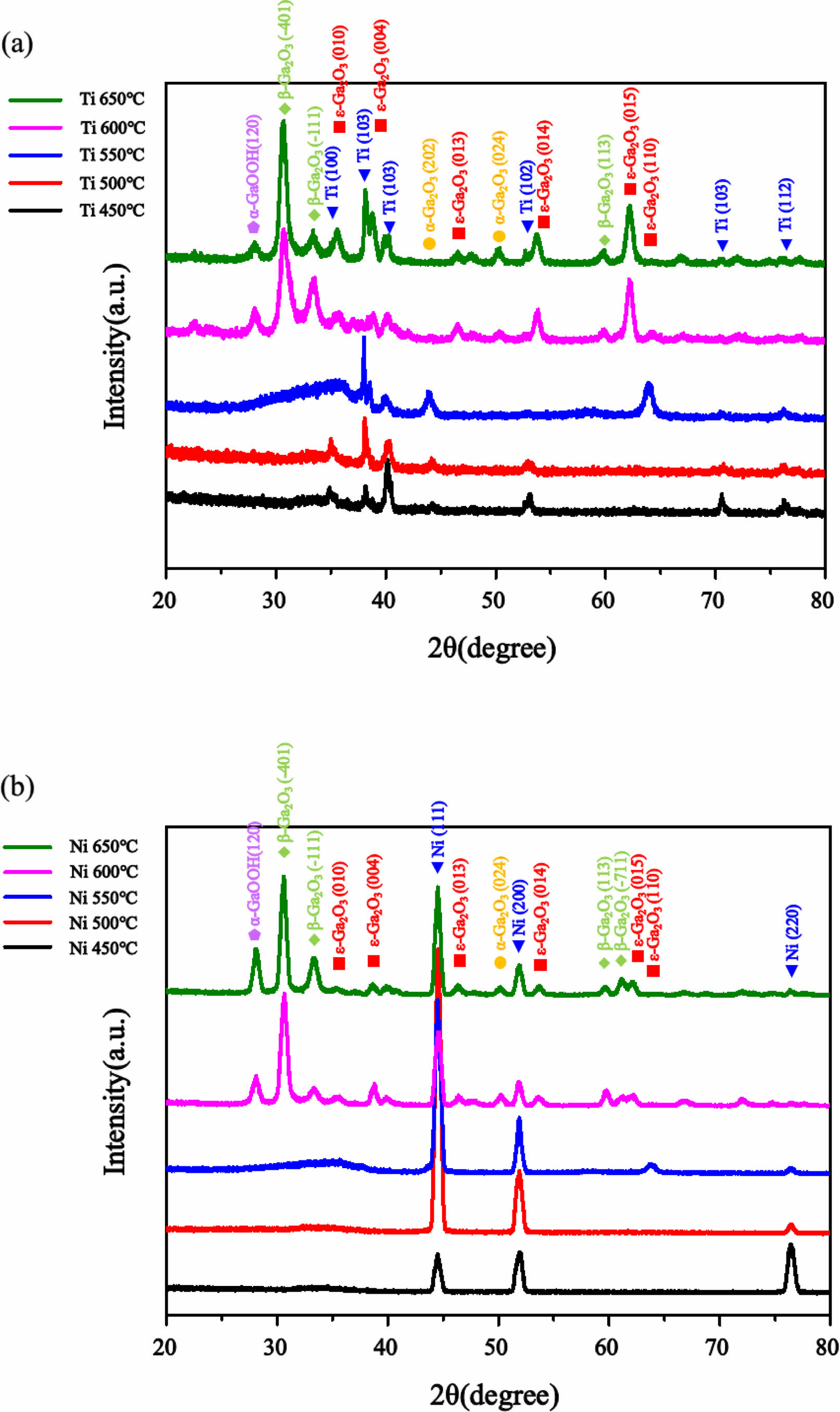
Fig. 1 shows diffraction patterns obtained through GIXRD measurements for thin films grown on Ti and Ni substrates at temperatures ranging from 450 to 650 °C. Samples grown at 450 °C, 500 °C, and 550 °C exhibited amorphous peaks in the range of 31° to 38° for both Ti and Ni substrates. Additionally, peaks originating from the metal substrates were observed. However, a weak α-Ga2O3 (202) peak was observed only when a Ti substrate was used. In the 550 °C sample, both substrates exhibited peaks corresponding to the ε-Ga2O3 (110) plane. This indicates that insufficient activation energy required for crystallization led to a predominant amorphous growth at temperatures below 500 °C. Crystallization began to occur within a specific temperature range of 500 °C to 550 °C. At higher growth temperatures of 600 °C and 650 °C, more progressed crystallization occurred and resulted in multiple peaks corresponding to various crystal α, ε, and β-Ga2O3 orientations. Furthermore, a GaOOH (120) peak was observed, which was attributed to using an H2O bubbling system.
Surface topography and growth characteristics
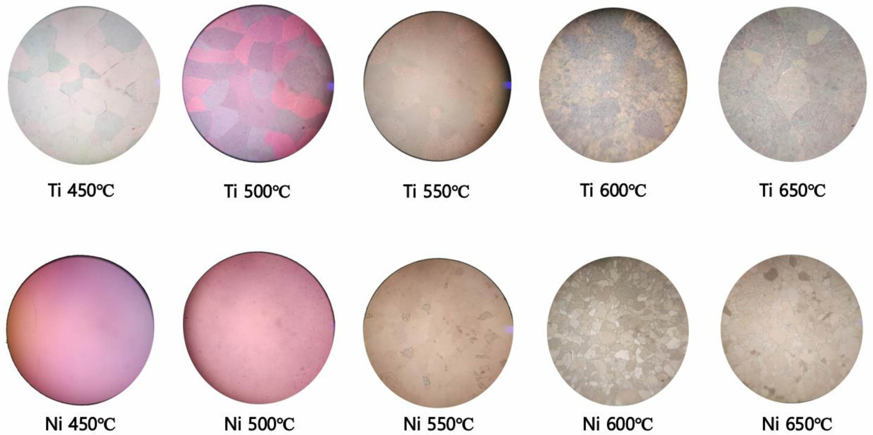
Fig. 2 shows the optical microscope images of samples grown at each temperature. In the case of thin films grown at temperatures ranging from 450 to 500 °C, it was observed that the film surfaces were relatively smooth and exhibited a pronounced interference-based reflective color. However, as the growth temperature increased, the color became less distinct. The cause of this is determined to be the increasing roughness of the surface at higher growth temperatures, as indicated by the SEM images, which will be further discussed later in Fig. 3 and 4. Additionally, both the Ti and Ni substrates exhibited a polycrystalline structure with an average grain length of 69.2 μm for Ti substrates and 32.7 μm for Ni substrates.
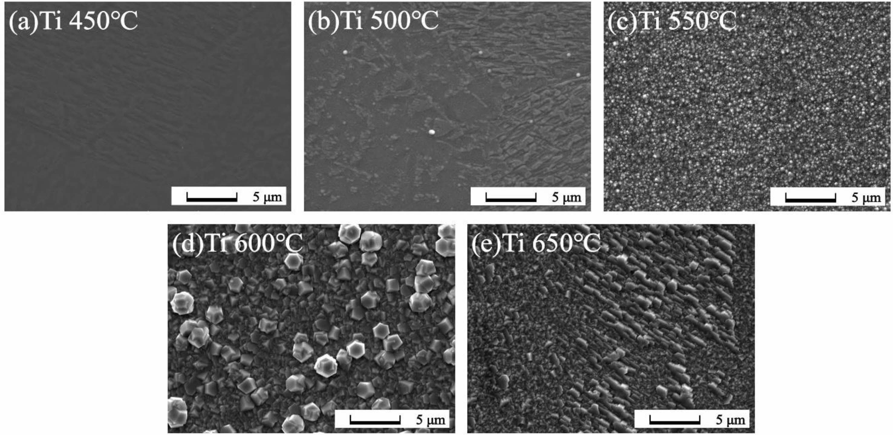
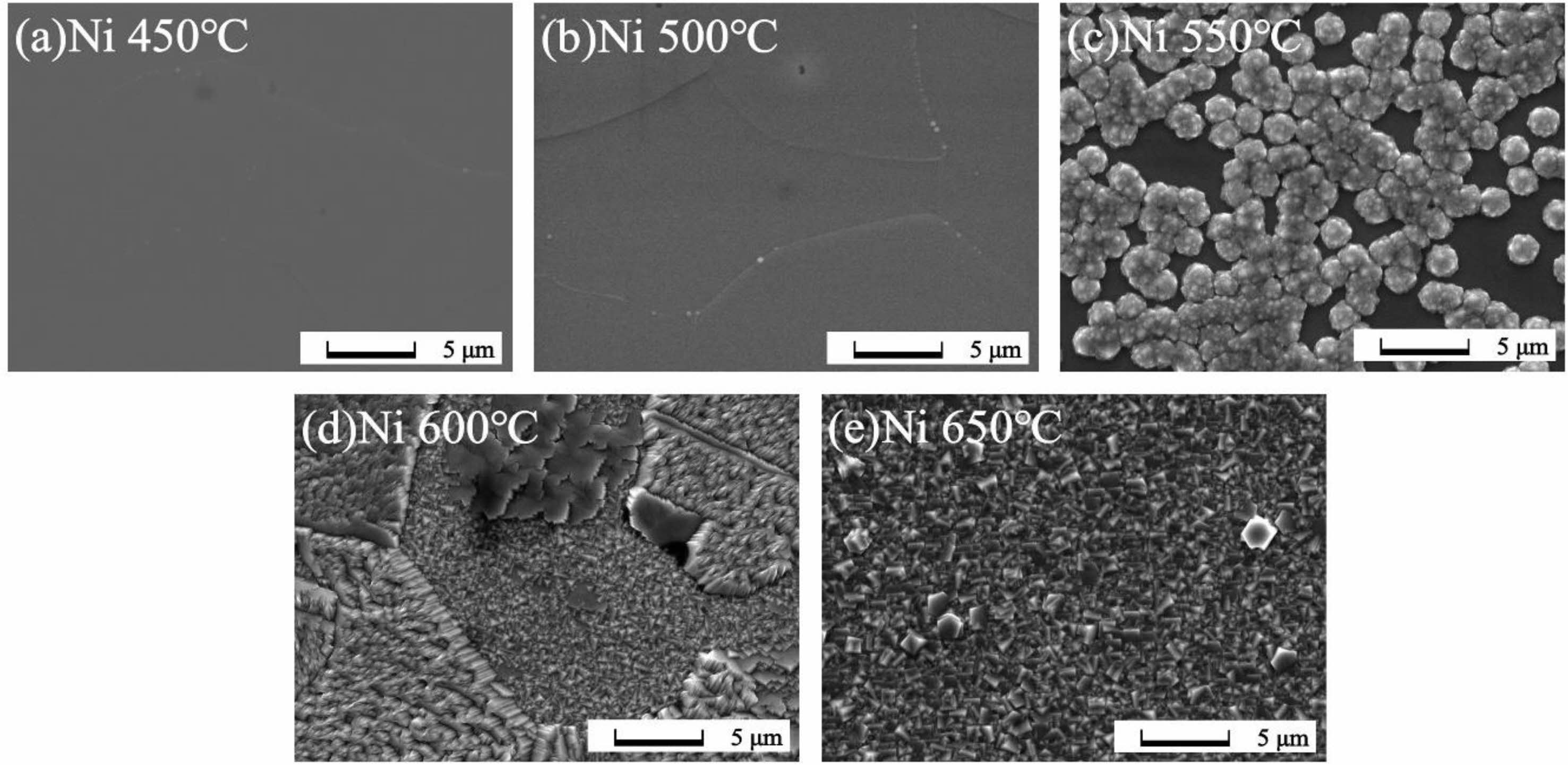
Fig. 3 and 4 show SEM images of the surfaces of the thin films grown at various temperatures. The samples grown at 450 °C and 500 °C show amorphous thin film structures on both the Ti and Ni substrates. As the growth temperature increases, the samples grown at 550 °C exhibit the onset of crystallization. On the Ti substrate, particles form on the surface, while on the Ni substrate, a cluster pattern is observed, composed of individual grains covering the surface. For samples grown at 600 °C and 650 °C, complete crystallization is observed, along with domains which shows diverse micro-crystalline shapes. These morphological results matched the GIXRD analyses, which showed that crystallization occurred minimally at growth temperatures below 500 °C, and the surface morphology was relatively smooth compared to samples grown at higher temperatures. As the growth temperature increases, crystallization occurs, leading to a tendency for the overall surface state to become rougher. This is speculated to be due to differences in surface diffusion and binding energies related to each grain, resulting in independent growth mechanisms of thin films for each grain [22]. Another factor that could contribute to the rough surface is the occurrence of changes in phase during grain generation or removal, potentially influenced by physical factors such as nano-sized grain boundary facets and internal defects within the grains [23]. Observed differences in surface morphology between the Ga2O3 thin films grown on Ti and Ni substrates was ascribed to the differences in lattice mismatch, the thermal expansion coefficient (TEC), and the strain release mechanism of Ga2O3 on different substrates. Additionally, according to the literature, it is known that diffusion of metal or metal oxide into the oxide thin film affects grain size and density shape. It is believed that the surface roughness and shape of the grains were also affected by the difference in the effect of interdiffusion of Ni (or NiO), Ti (or TiO2), and Ga2O3 on grains at each growth temperature [24, 25].
Current-voltage characteristics of the MOM structures
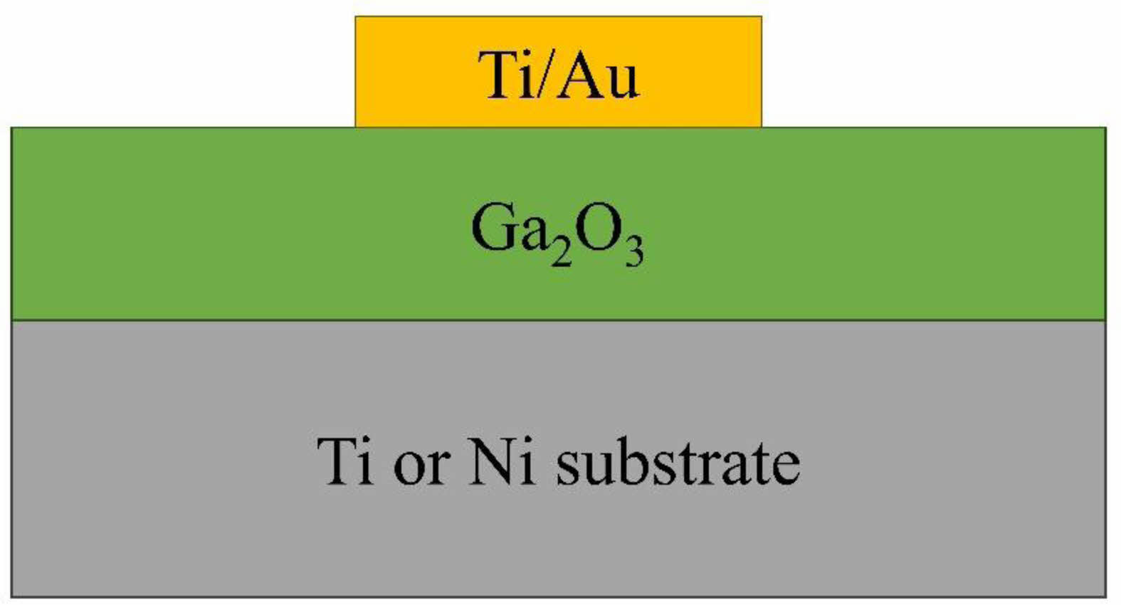
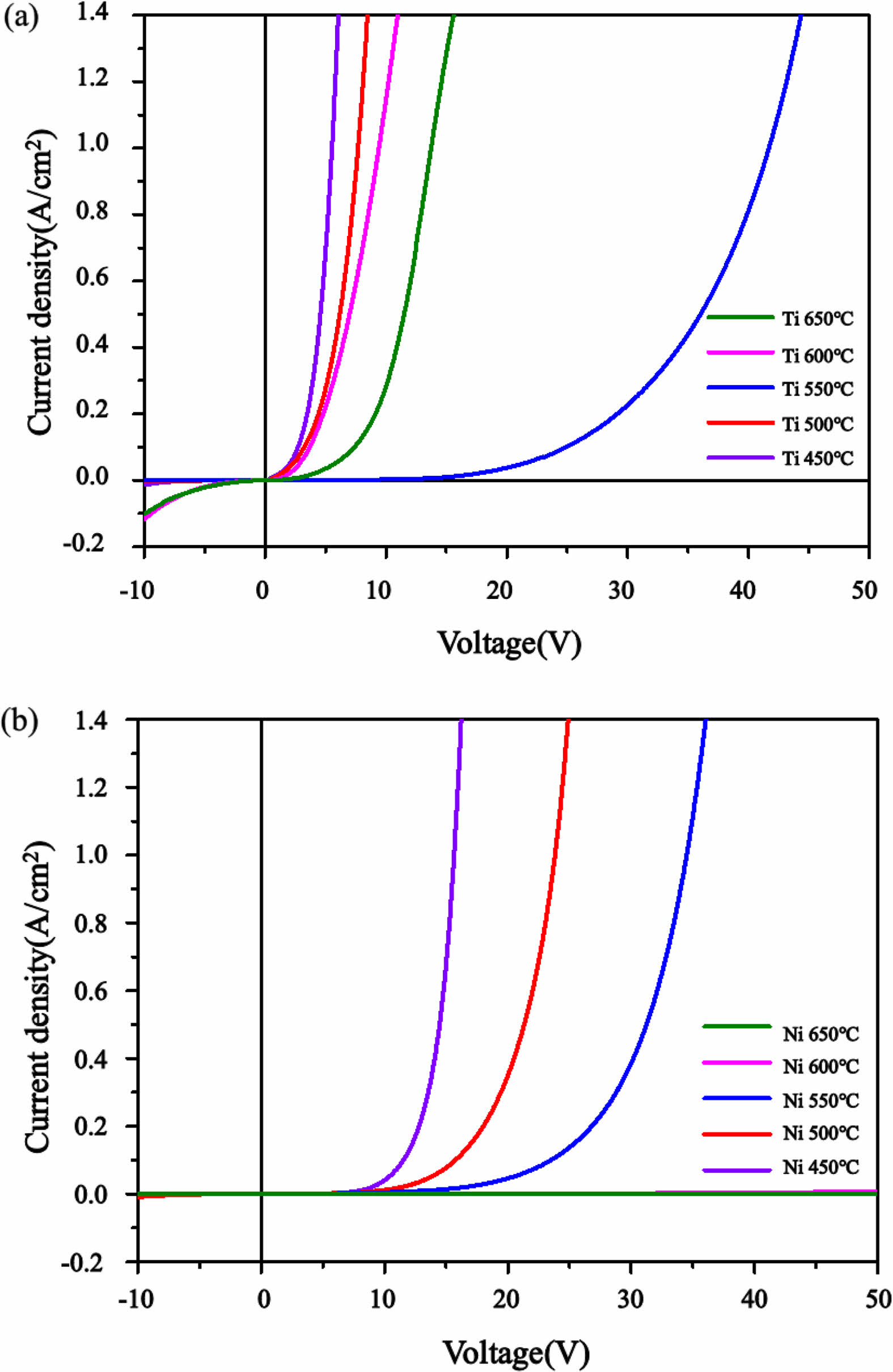
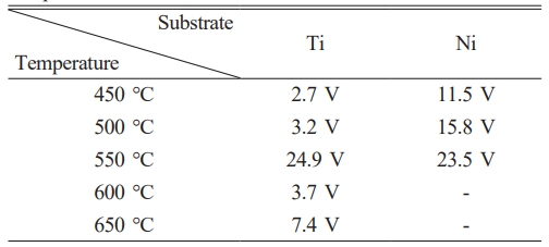
In order to examine the electrical characteristics of thin films, vertical metal-oxide-metal (MOM) structures were fabricated by depositing Ti/Au (50 nm/50 nm) electrodes with a diameter of 300 μm onto Ga2O3 thin films grown at various temperatures using an e-beam evaporator. A schematic view of the metal-oxide-metal (MOM) structure is shown in Fig. 5, and the current-voltage characteristics are shown in Fig. 6. Regardless of the substrate or growth temperature, the samples exhibit higher operating voltages compared to conventional Si or SiC diodes [26-29]. The operating voltages at 0.1A/cm² for each condition are presented in Table 1. For both Ti and Ni substrates, as the growth temperature increases to 450 °C, 500 °C, and 550 °C, the operating voltage also increases, showing a gentle slope with increasing current. In the case of Ti substrates grown at higher temperatures of 600 °C and 650 °C, the leakage current increases in the reverse bias region, and the operating voltage is significantly lower than that of the 550 °C sample. However, Ni substrates exhibit high resistance and minimal current flow even at high voltages. It can be observed that Ni substrates exhibit higher operating voltages compared to Ti substrates at growth temperatures ranging from 450 to 550 °C. In this experiment, oxygen is introduced first by bubbling H2O during the growth of Ga2O3 thin films. This can lead to the formation of oxide films in the Ti and Ni substrates, and the difference in operating voltage depending on the substrate can be attributed to the following two factors: (1) NiO has a larger bandgap compared to TiO2 (NiO: 3.6-4.6 eV, TiO2: 3.2 eV), (2) Differences in the thickness of the oxide layer formed due to the higher reactivity of oxygen with titanium compared to nickel may result in variations in tunneling current, consequently leading to an increase in the operating voltage difference. In the case of Ti substrates, there is a noticeable rise in operating voltage at 550 °C. At present, there is speculation that the sudden variation in oxide film thickness is a key factor, but additional research is required, encompassing aspects such as carrier re-trapping and scattering resulting from crystallites formed during the initial stages of crystallization. Research in this area will be a continual effort in the future. In addition, both at 600 °C and 650 °C, Ti substrates display significant leakage current and a decrease in operating voltage in the reverse bias region. It is hypothesized that the reason for this phenomenon is the enhanced interaction between the substrate and the thin film at elevated growth temperatures in the case of Ti substrates, as opposed to Ni substrates, resulting in the creation of paths for electrical leakage. Despite the smaller average grain size of Ni compared to Ti, suggesting a higher density of grain boundaries in the electrode region and potential for larger leakage current through grain boundaries in Ni substrates, the experimental findings demonstrate that Ti substrates exhibit higher leakage current. This indicates the potential for different leakage current paths extending beyond the density of grain boundaries. Therefore, when utilizing metal substrates for the deposition of Ga2O3 thin films, it is imperative to thoroughly examine and evaluate not just the impact of grain boundaries but also the growth mechanisms within individual grains, alterations at the interface caused by temperature during heat treatment, and the energy required for the activation of impurities or traps.
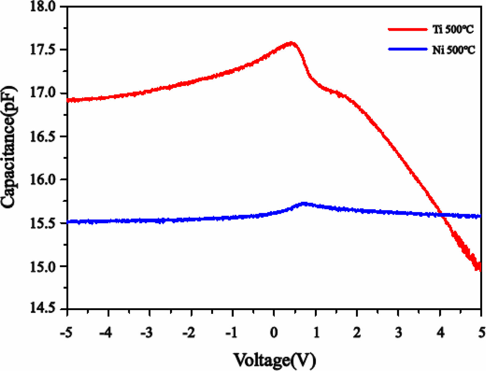
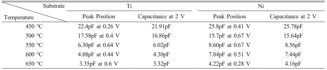
Capacitance-voltage characteristics were measured at a frequency of 1 MHz, and the peak positions and representative values of the capacitance at 2 V for the entire temperature range are summarized in Table 2. In Fig. 7, the results for thin films grown at 500 °C are presented to compare the characteristics of Ti and Ni substrates. Capacitance peaks are commonly observed within the range of 0-1 V. The presence of peaks within the range of 0-1 V can be explained by various factors, including high series resistance, interfacial states and layers forming during electrode and thin film deposition, imperfect ohmic contacts, or surface traps [30-34].
In case of MOSFETs, for an example, those characteristics of the capacitance can have negative effects such as unstable threshold voltage and deterioration of frequency response characteristics on the device due to parasitic capacitance, so the occurrence of these defects must be minimized.
The Ti substrates exhibit a more abrupt change in response to voltage variations compared to the Ni substrates. In the reverse bias region, there was initially an increase in capacitance, followed by a peak approximately around 0-1 V, and then a shoulder peak occurred near 2 V. On the other hand, for the forward bias, the capacitance values showed a tendency to decrease. Hence, it is possible to speculate that the Ga2O3 thin film on Ti substrates exhibits a greater variety of traps than Ni substrates. The occurrence of these traps may be affected by the polycrystalline nature of the thin film, grain boundaries, and interfacial states on the surface. It is postulated that multiple pathways are involved in the formation of these traps within the Ga2O3 thin film on Ti substrates, compared to Ni substrates [30]. Capacitance values were found to vary from a few pF to several tens of pF, and an increase in growth temperature for both Ti and Ni substrates resulted in a decrease in capacitance values. According to the I-V characteristics, changes in capacitance values depend on the growth temperature can be attributed to various factors, including the trapping of carriers during the transition from amorphous to crystalline states and scattering at grain boundaries.
|
Fig. 1 XRD diffraction patterns of Ga2O3 thin films depend on growth temperature and metallic substrate (a) Ti and (b) Ni. |
|
Fig. 2 Microscopic optical images of Ga2O3 thin films depend on growth temperature and metallic substrates. |
|
Fig. 3 SEM images of Ga2O3 thin films grown on Ti substrates according to growth temperatures (a) 450 ℃, (b) 500 ℃, (c) 550 ℃, (d) 600 ℃, (e) 650 ℃. |
|
Fig. 4 SEM images of Ga2O3 thin films grown on Ni substrates according to growth temperatures (a) 450 ℃, (b) 500 ℃, (c) 550 ℃, (d) 600 ℃, (e) 650 ℃. |
|
Fig. 5 Schematic view of the metal-oxide-metal (MOM) structures to evaluate electrical properties. |
|
Fig. 6 I-V characteristics of Ga2O3 Schottky diodes depend on growth temperature and metallic substrates (a) Ti and (b) Ni. |
|
Fig. 7 C-V characteristics of Ga2O3 vertical diodes depend on growth temperature and substrate. Ti (red line), Ni (blue line). |
|
Table 1 Operating voltages (at 0.1 A/cm2 ) depend on growth temperature and substrate. |
|
Table 2 C-V characteristics of Ga2O3 vertical diodes depend on growth temperature and substrate |
In this study, Ga2O3 was grown on Ti and Ni substrates using MOCVD with a fixed flow rate across a range of temperatures (450 °C to 650 °C). Vertical metal-oxide-metal (MOM) structures were fabricated on the thin film surface using Ti electrodes and their electrical properties were analyzed. Amorphous thin films were formed at relatively low temperatures of 450 °C and 500 °C. Crystallization began at 550 °C, and crystalline α, ε, and β-Ga2O3 thin films were formed at 600 °C and 650 °C. It was observed that as crystallization progressed, the surface became rough, likely due to factors such as surface diffusion on grain boundaries, differences in binding energy, and variations in mobility during the crystallization process. The I-V measurements revealed that for both Ti and Ni substrates, in the temperature range of 450 °C to 550 °C, as the growth temperature increased, there was an increasing trend in the operating voltage. However, at 600 °C and 650 °C, it was observed that on the Ti substrates, leakage current increased in the reverse bias region, and operating voltage decreased, while on the Ni substrates, there was almost no current flow. The analysis of these characteristics implies that when exposed to higher temperatures, titanium substrates exhibit a stronger interaction with the thin film compared to nickel substrates, resulting in the generation of paths for leakage current. Peaks were observed in the C-V analysis which could be attributed to high series resistance, interfacial states, and interfacial layers. Additionally, it was observed that the capacitance decreased with increasing growth temperature. Through a comparative analysis of capacitance trends, it can be observed that the Ti substrate has a significantly higher impact on the creation of traps within the Ga2O3 thin films, when compared to the Ni substrate. The observed differences in capacitance values at varying growth temperatures are speculated to be influenced by several factors, including carrier trapping and scattering at grain boundaries, during the transition from the amorphous to the crystalline phase. Lastly, although this study has only concentrated on metallic substrates composed of Ni and Ti, forthcoming investigations will explore a broader range of metal substrates and conduct related experiments. Concurrently, further investigations, such as transmission electron microscopy (TEM) and secondary ion mass spectrometry (SIMS), will be performed to gather more accurate data on the interface state between the metal substrates and Ga2O3 layers. The characteristics of demonstrating high operational performance in the range of 10 V~20 V are expected to be applied using TVS or varistor components, which can protect the device in the intermediate voltage region rather than at high voltages. However, in order to take maximum advantages of Ga2O3's excellent material properties (including: large energy bandgap, high breakdown voltage, etc.), it is necessary, as further works, to establish thin film growth conditions that minimize defects between the metal substrate and the Ga2O3 thin films.
This research was supported by the Korea Institute for Advancement of Technology (KIAT) grant funded by the Korea Government (MOTIE) (P0012451, The Competency Development Program for Industry Specialist). Also, this research was partially supported by the Korea Evaluation Institute of Industrial Technology (KEIT) grant funded by the Korea government (MOTIE) (RS-2022-00154720, Technology Innovation Program Development of next-generation power semiconductor based on Si-on-SiC structure).
- 1. A. Kumar, M. Moradpour, M. Losito, W.-T. Franke, S. Ramasamy, R. Baccoli, and G. Gatto, Energies 15[23] (2022) 9172.
-

- 2. D. Garrido-Diez, and I. Baraia, Proc. IEEE Int. Workshop Electron. Control Meas. Signals Their Appl. Mechatronics (ECMSM). (2017) 1-6.
-
- 3. J. Millan, P. Godignon, X. Perpiñà, A. Pérez-Tomás, and J. Rebollo, IEEE Trans. Power Electron. 29[5] (2014) 2155-2163.
-
- 4. M. Orita, H. Ohta, M. Hirano, and H. Hosono, Appl. Phys. Lett. 77[25] (2000) 4166-4168.
-
- 5. M. Higashiwaki, K. Sasaki, A. Kuramata, T. Masui, and S. Yamakoshi, Phys. Status Solidi A 211[1] (2014) 21-26.
-
- 6. A.B. Yönetken and A. Yönetken, J. Ceram. Process. Res. 25[1] (2024) 97-103.
-
- 7. J.H. Hwang and K.-T. Lee, J. Ceram. Process. Res. 21[2] (2020) 148-156.
-
- 8. I. Jeon, J.H. Hwang, T.G. Kim, L. Yin, H.W. Lee, J.P. Kim, H.S. Ahn, and C.R. Cho, J. Ceram. Process. Res. 22[2] (2021) 192-199.
-
- 9. H.F. Mohamed, C. Xia, Q. Sai, H. Cui, M. Pan, and H. Qi, J. Semicond. 40[1] (2019) 011801.
-
- 10. M. Higashiwaki, AAPPS Bull. 32[1] (2022) 3.
-
- 11. M. Handwerg, R. Mitdank, Z. Galazka, and S.F. Fischer, Semicond. Sci. Technol. 30[2] (2015) 024006.
-
- 12. P. Jiang, X. Qian, X. Li, and R. Yang, Appl. Phys. Lett. 113[23] (2018) 232105.
-
- 13. S.J. Pearton, J. Yang, P.H. Cary, F. Ren, J. Kim, M.J. Tadjer, and M.A. Mastro, App. Phys. Rev. 5[1] (2018) 011301.
-
- 14. Z. Guo, A. Verma, X. Wu, F. Sun, A. Hickman, T. Masui, A. Kuramata, M. Higashiwaki, D. Jena, and T. Luo, Appl. Phys. Lett. 106[11] (2015) 111909.
-
- 15. P. Sittimart, S. Ohmagari, T. Matsumae, H. Umezawa, and T. Yoshitake, AIP Adv. 11[10] (2021) 105114.
-
- 16. G. Joshi, Y.S. Chauhan, and A. Verma, J. Alloys Compd. 883 (2021) 160799.
-
- 17. Y. Song, P. Ranga, Y. Zhang, Z. Feng, H.-L. Huang, M.D. Santia, S.C. Badescu, C.U. Gonzalez-Valle, C. Perez, K. Ferri, R.M. Lavelle, D.W. Snyder, B.A. Klein, J. Deitz, A.G. Baca, J.P Maria, B. Ramos-Alvarado, J. Hwang, H. Zhao, X. Wang, S. Krishnamoorthy, B.M. Foley, and S. Choi, ACS Appl. Mater. Interfaces 13[32] (2021) 38477-38490.
-
- 18. P. Yan, Z. Zhang, Y. Xu, H. Chen, D. Chen, Q. Feng, S. Xu, Y. Zhang, J. Zhang, C. Zhang, and Y. Hao, Vacuum. 204 (2022) 111381.
-
- 19. N. Nepal, D.S. Katzer, B.P. Downey, V.D. Wheeler, L.O. Nyakiti, D.F. Storm, M.T. Hardy, J.A. Freitas, E.N. Jin, D. Vaca, L. Yates, S. Graham, S. Kumar, and D.J. Meyer, J. Vac. Sci. Technol. A 38[6] (2020) 063406.
-
- 20. S.A.O. Russell, A. Pérez-Tomás, C.F. McConville, C.A. Fisher, D.P. Hamilton, P.A. Mawby, and M.R. Jennings, IEEE J. Electron Devices Soc. 5[4] (2017) 256-261.
-
- 21. N.J. Ahn, J.B. An, H.S. Ahn, K.H. Kim, and M. Yang, J. Korean Cryst. Growth Cryst. Technol. 33[4] (2023) 125-131.
-
- 22. S.B. Lee, D.Y. Yoon, N.M. Hwang, and M.F. Henry, Metall. Mater. Trans. A. 31 (2000) 985-994.
-
- 23. J. Zhang, W. Ludwig, Y. Zhang, H.H.B. Sørensen, D.J. Rowenhorst, A Yamanaka, P.W. Voorhess, and H.F. Poulsen, Acta Mater. 191 (2020) 211-220.
-
- 24. A.C. Caballero, J.F. FernBndez, C. Moure, and P. Duriin, J. Eur. Ceram. Soc. 17[4] (1997) 513-523.
-
- 25. Y.-C. Lee, H.-J. Hsu, I.-Y. Huang, H.-J. Shih, and C. Pithan, J. Ceram. Process. Res. 24[6] (2023) 992-1000.
-
- 26. S.J. Kim, D.J. Oh, S.J. Yu, and Y.D. Woo, J. Korean Phys. Soc. 49[9] (2006) 768-773.
- 27. A.R. Hefner, R. Singh, J.S. Lai, D.W. Berning, S. Bouche, and C. Chapuy, IEEE Trans. Power Electron. 16[2] (2001) 273-280.
-
- 28. M.K. Parida, S.T. Sundari, V. Sathiamoorthy, and S. Sivakumar, Nucl. Instrum. Methods Phys. Res., Sect. A 905 (2018) 129-137.
-
- 29. X. Deng, L. Yang, Y. Wen, X. Li, F. Yang, H. Wu, H. Cao, J. Li, W. Chen, and B. Zhang, Superlattices Microstruct. 138 (2020) 106381.
-
- 30. Alisha, P. Chander, V.K. Malik, and R. Chandra, J. Phys.: Conf. Ser. 2518[1] (2023) 012016.
-
- 31. B. Bati, Ç. Nuhoğlu, M. Sağlam, E. Ayyildiz, and A. Türüt, Phys. Scr. 61[2] (2000) 209.
-
- 32. X. Wu and E. S. Yang, J. Appl. Phys. 65[9] (1989) 3560-3567.
-
- 33. P. Chattopadhyay and B. Raychaudhuri, Solid-State Electron. 35[7] (1992) 1023-1024.
-
- 34. B. Şahin, H. Çetin, and E. Ayyildiz, Solid State Commun. 135[8] (2005) 490-495.
-
 This Article
-
2024; 25(3): 439-445
Published on Jun 30, 2024
- 10.36410/jcpr.2024.25.3.439
- Received on Apr 4, 2024
- Revised on May 28, 2024
- Accepted on May 29, 2024
Services
- Abstract
introduction
experiment
result and discussion
conclusion
- Acknowledgements
- References
- Full Text PDF
Shared
Correspondence to
- Min Yang
-
Department of Nano Semiconductor Engineering, Korea Maritime and Ocean University, Busan 49112, Korea
Tel : +82-10-3648-2551 Fax: +82-51-404-3986 E-mail: myang@kmou.ac.kr - E-mail: myang@kmou.ac.kr
Clean-Energy Research Institute(CRI), Hanyang University, 222, Wangsimni-ro, Seongdong-gu, Seoul, 04763, Korea
E-mail: jcpr@hanyang.ac.kr