


- The dielectric and electrical modulus properties of Ba(Al0.5Nb0.5)xTi1-xO3 ceramics
R.F. Niu, D.P. Wang, Z.H. Huang, and W.T. Wang*
School of Physics and Electronic Information, Yantai University, Yantai 264005, P.R. China
This article is an open access article distributed under the terms of the Creative Commons Attribution Non-Commercial License (http://creativecommons.org/licenses/by-nc/4.0) which permits unrestricted non-commercial use, distribution, and reproduction in any medium, provided the original work is properly cited.
In this work, a series of BaTiO3-based ceramic materials, Ba(Al0.5Nb0.5)xTi1-xO3 (x = 0, 0.04, 0.06, 0.08), was synthesized using a standard solid-state reaction technique. In the temperature range of 100~380 K, the frequency-dependent dielectric and electrical modulus properties were studied. A colossal dielectric permittivity (>1.5×10⁴) and low dielectric loss (< 0.01) were demonstrated at the optimal doping concentration x = 0.04. The observed dielectric behavior of Ba(Al0.5Nb0.5)xTi1-xO3 ceramics can be attributed to the Universal Dielectric Response. The complex electrical modulus spectra indicate a significant decrease in capacitance and permittivity of the grains with increasing co-doping concentration. Our results provide insight into the role of donor and acceptor co-doping on the properties of BaTiO3-based ceramics, which is important for their use in dielectric and energy storage applications.
Keywords: Ceramics, Colossal permittivity, Dielectric properties, Complex modulus analysis.
Ferroelectric and dielectric materials have gained popularity due to their unique features and prospective uses in a variety of fields, including sensors, capacitors, data storage, and energy harvesting [1, 2]. Among them, BaTiO3-based ceramics have been widely studied in the past decade for the purpose to acquire high dielectric constant, strong piezoelectricity, and good thermal stability [3-6]. However, to further enhance their targeted properties, doping elements with different valence states into BaTiO3 has been proved to be an effective and practicable way [7-9]. In particular, the B-site doping with quadrivalent and trivalent elements has been reported to have a significant impact on the dielectric, ferroelectric and piezoelectric properties of BaTiO3-based ceramics because of the known localized lattice defect states [10].
According to a literature conducted by Lee et al., it was observed that with the increase of doping concentration
of Al, the Curie point of Ba(Ti1-xAlx)O3 showed a downward shift to lower temperatures, and the dielectric constants exhibited a reduction at low frequencies [11]. Cao et al. reported the dielectric behavior of Nb-doped Ba(ZrxTi1−x)O3 ceramics, and effect of the variation of Nb2O5 content and sintering temperature on the dielectric constant was explained [12]. A recent literature reported the dielectric properties of Fe-doped BaTi0.8Sn0.2O3 ceramics, and the defect dipoles and nano-polar regions originated from the coexistence of Fe2+ and Fe3+ were shown to influence the permittivity, the Curie temperature and the dielectric tenability [13].
Under normal conditions, the valence state of Al is +3, while that of Nb is +5. Co-doping with Al and Nb ions into BaTiO3 are expected to develop high performance of dielectric properties and elicit relaxation phenomena due to the presence of localized defect dipoles. In this work, Ba(Al0.5Nb0.5)xTi1-xO3 ceramics with x = 0, 0.04, 0.06, and 0.08 were synthesized via a standard high-temperature solid-state reaction method. The low-temperature dielectric and electrical modulus characteristics of the prepared specimens were investigated. The temperature and frequency dependence of the grain and grain boundary responses also analyzed. The purpose of this study is to evaluate the possibility of (Al, Nb) co-doping to modify the properties of BaTiO3 ceramics and to determine the optimal doping concentration to achieve a high dielectric constant and low dielectric loss, which can carry significant implications for their prospective utilization in piezoelectric and energy storage devices.
The ceramic Ba(Al0.5Nb0.5)xTi1-xO3 (BTNA) samples were synthesized by employing titanium dioxide (TiO2), barium carbonate (BaCO3), aluminum oxide (Al2O3), and niobium pentoxide (Nb2O5) as the precursor ingredients. Four samples were created by assigning x values to x = 0, 0.04, 0.06, and 0.08, specifically, and the corresponding samples were labeled as BTNA00, BTNA04, BTNA06, and BTNA08, respectively. The stoichiometric powders were measured using an electronic precision balance and thoroughly blended and milled to create a homogeneous mixture. This combination was then transferred into an alumina crucible and subjected to a Muffle furnace pre-sintering at a temperature of 1250 ℃ for 4 hours, resulting in the synthesis of BTNA powders. The ground powders were inserted into a cylindrical matrix and subjected to uniaxial pressing at a pressure of 14 MPa. This process resulted in the formation of 10-diameter pellets with a thickness of 3 mm. Subsequently, these pellets were sintered at a temperature of 1300 ℃ for 10 hours, leading to the formation of BTNA ceramic samples.
The samples' crystal structure was examined using an X-ray diffractometer (XRD, Bruker D8-A25). A source of Mg-Kα radiation was employed in X-ray photoelectron spectroscopy (XPS, VGESCALab-5) to investigate the chemical states of the chemical components.The dielectric properties were studied using a QuadTech 1730 LCR digital bridge within the frequency range of 100 Hz to 100 kHz. The electrical modulus spectrum was recorded using an HP4194A analyzer. The data were collected in the temperature range of 380 K to 100 K.
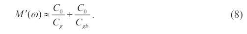
Figure 1 shows the XRD patterns of the prepared samples. The peaks marked with diamonds are related to the tetragonal perovskite phase matched well with the PDF Card No. 05-0626. The results indicate that a small amount of Al+Nb co-doping into BaTiO3 does not change the crystal structure significantly. As the doping concentration increases to x = 0.08, weak secondary phases marked with circles for BTNA08 are related to polycrystalline structure of Nb12O29 matched well with the PDF Card No. 34-1169. Fig. 1(b) shows the location of the strongest diffraction peaks of the samples.
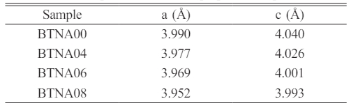
It is clear that when doping concentration increases, the peak shifts slightly in the direction of the high angle, indicating a reduction in the lattice parameters. The determined lattice constants for the samples are listed in Table 1. As is known, there is little difference between the size of Ti4+ (~61 pm) and Nb5+ (~63 pm), while the radius of Al3+ ion is about 53.5 pm. It is doping with smaller ions that causes the lattice constant to drop.
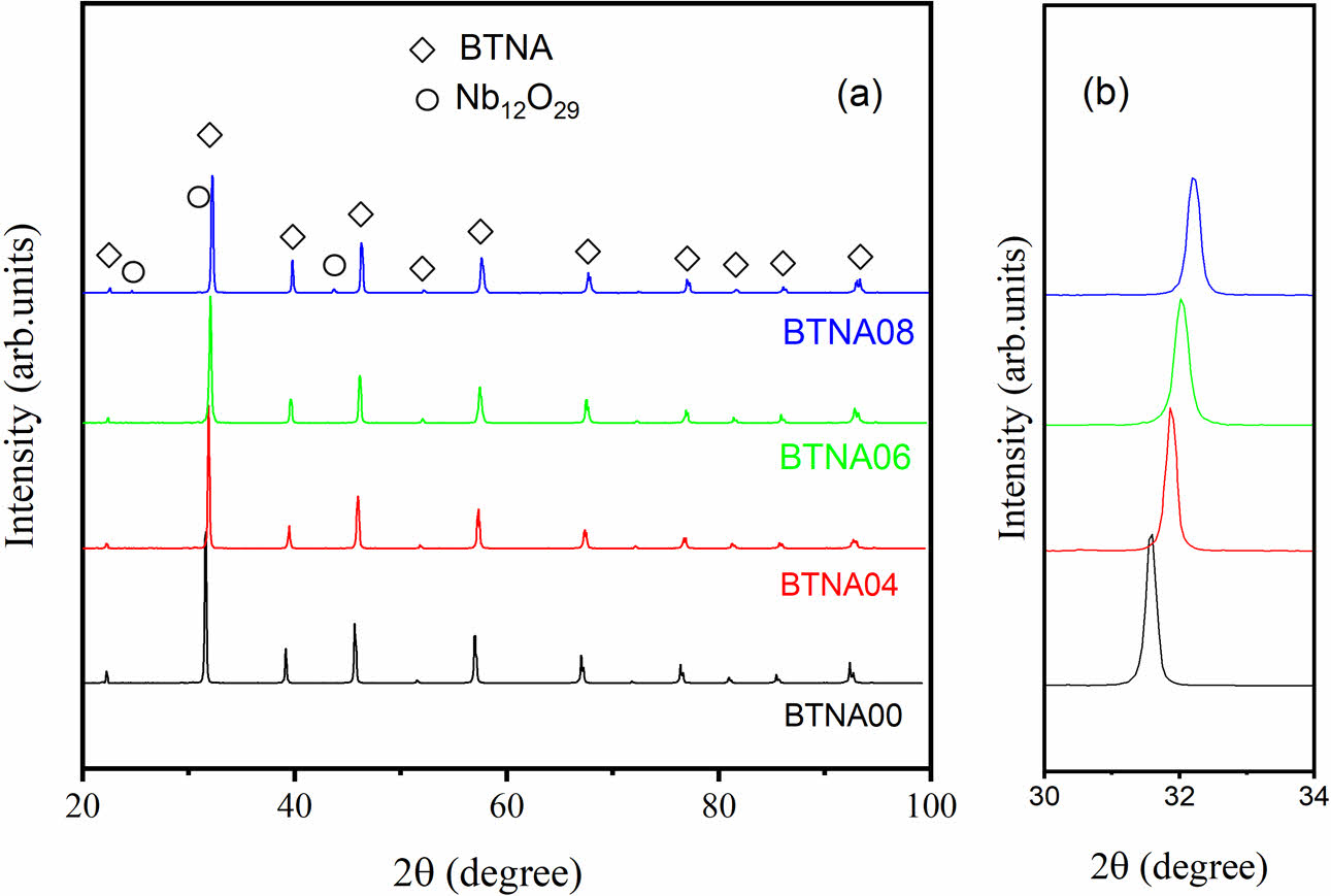
XPS data were recorded to illustrate the chemical state of the elements for the BTNA samples. All the samples show roughly the same spectra, which suggest the identical chemical state of the component elements in the BTNA samples. Typical results for BTNA04 are shown in Fig. 2. The Ba 3d5/2 and 3d3/2 peaks [Fig. 2(a)] are observed at 779.8 and 795.2 eV, respectively, revealing the presence of Ba2+. The Ti 2p3/2 and 2p1/2 peaks [Fig. 2(b)] locate at 459.0 and 465.2 eV, respectively, indicating the existence of Ti4+. The values of 207.6 eV (Nb 3d5/2) and 210.0 eV (Nb 3d3/2) [Fig. 3(c)] manifest the chemical state of Nb5+. The Al 2p peak [Fig. 3(d)] at 74.7 eV has closely-spaced spin-orbit components, which can be ignored for Al3+.
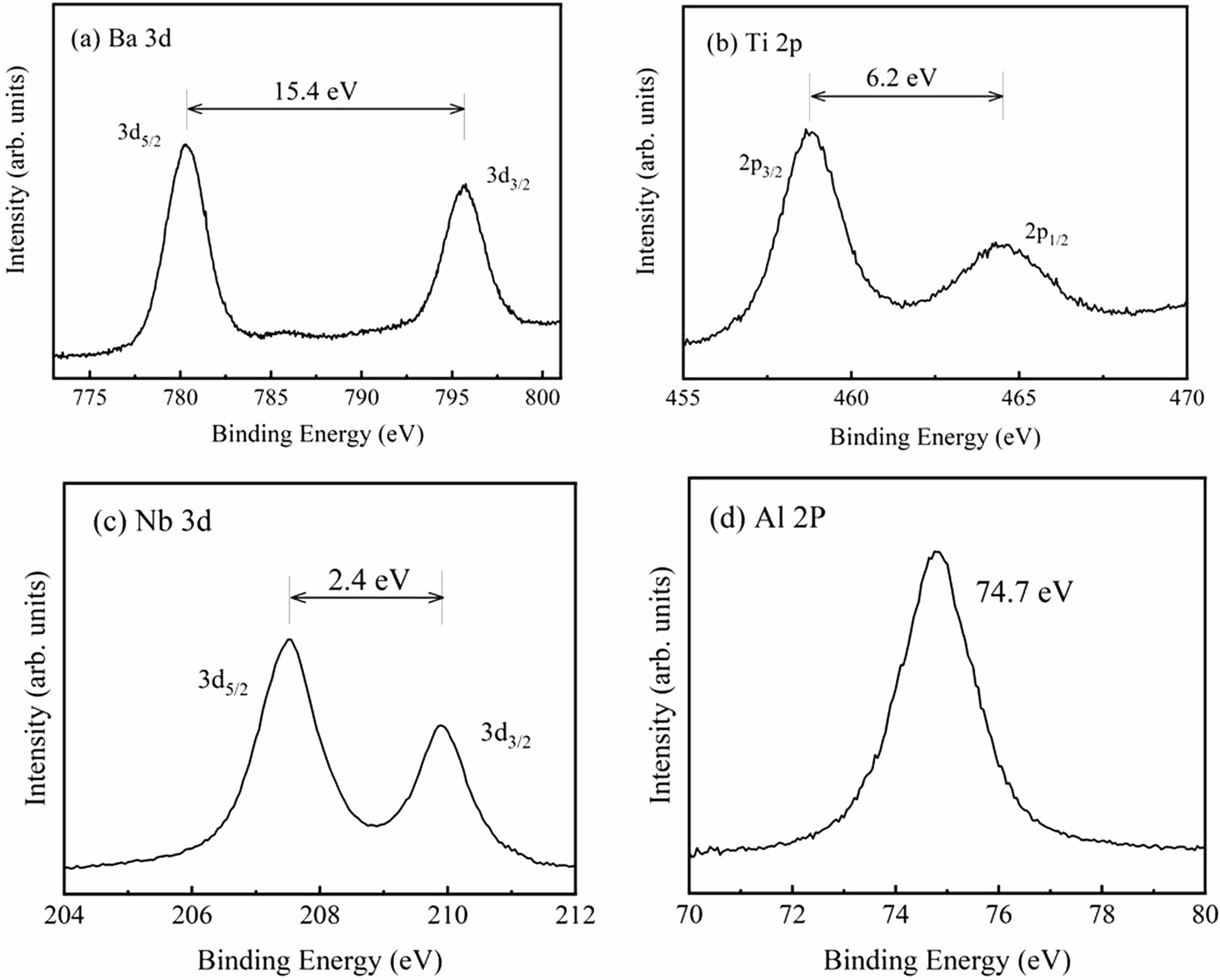
Figure 3 illustrates the variation of the dielectric constant ε′ and the loss tangent tanδ of the prepared samples as a function of temperature at 1 kHz. The peaks at near 300 K represent the typical phase transition of BaTiO3-based materials. It is obvious that Al+Nb co-doping contributes to the increase of dielectric constant [Fig. 3(a)] and the reduction of dielectric loss [Fig. 3(b)]. The maximum value of ε′ exceeds 15000, and the minimum value of tanδ is lower than 0.01 when the doping concentration is 4%. With further increase of the doping concentration, the dielectric constant ε′ decreases, and the phase transition shifts to a lower temperature. As for BTNA08, the doping concentration increases to 8%, the dielectric peak decreases and broadens. This is due to the fact that excessive Nb or Al dopants are located in the grain boundary region, resulting in a reduction in grain size and flattening the curves of BTNA08.
During the solid-state reaction, the cations Al3+ and Nb5+ were incorporated into the B-site, resulting in the formation of two distinct competing compensation mechanisms:
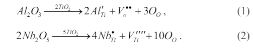
When Al is substituted for the B-site Ti, it can lead to the formation of a negatively charged ionic defect [AlTi′].
In order to compensate for this acceptor-type defect center, an oxygen defect [Vo ••] is created. In much the same way, when Nb is substituted for the Ti, it can lead to the formation of a positively charged ionic defect [NbTi]. In order to compensate for this donor-type defect center [NbTi], a Ti vacancy [VTi′′] is created. This results in the establishment of a local random electric field. The samples demonstrate a competitive interplay between long-range order and the local random field caused by Nb+Al doping. Defect clusters are widely recognized for their ability to generate local lattice stresses and random fields, resulting in the formation of polar nanoregions (PNRs) [14]. These PNRs are thought to play a significant role in the observed dielectric relaxation behavior. As the concentration of Nb increases, the emergence of a localized random field becomes evident, leading to the disruption of larger ferroelectric domains and the formation of PNRs, thereby reducing the degree of diffusion phase transition and relaxation behavior [as shown in Fig. 3(b)].
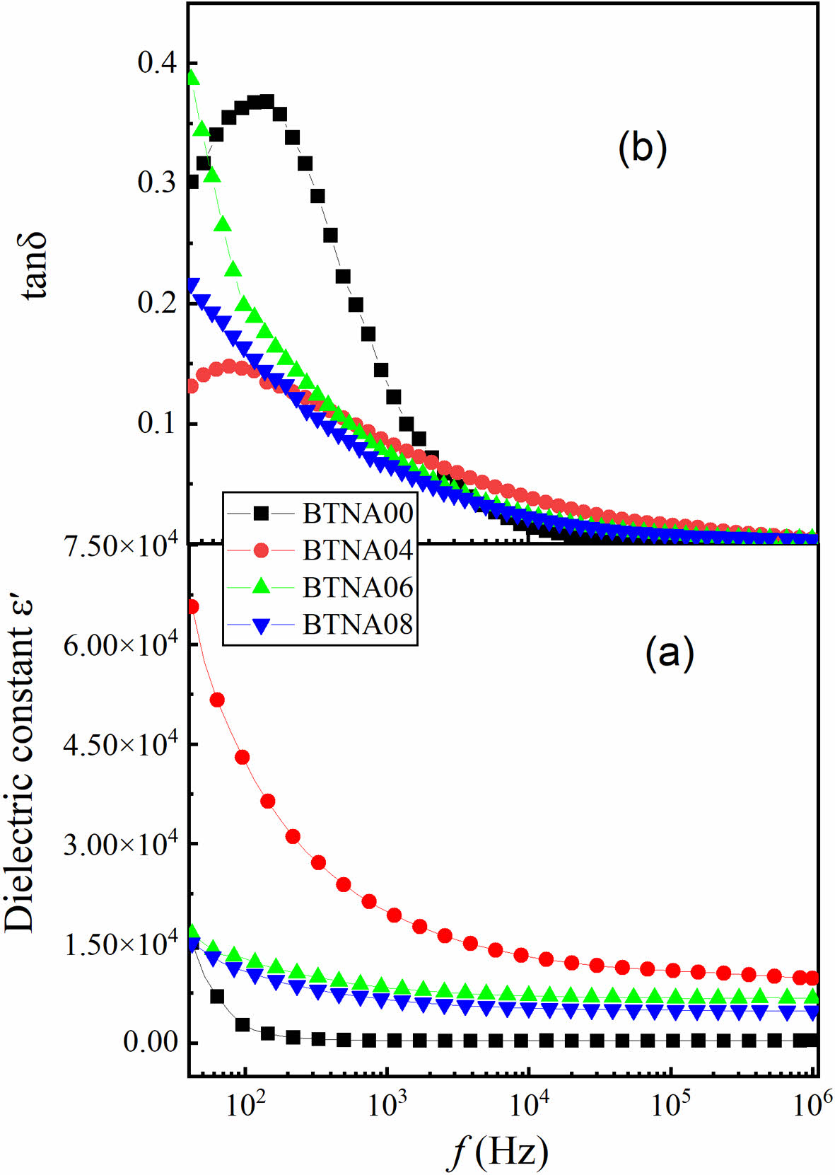
Figures 4(a) and 4(b) show the frequency dependence of ε′ and tanδ of BTNA ceramic samples at room
temperature, respectively. The weak frequency dependency of the dielectric constant can be seen in the doped samples, with the exception of BTNA04, and the values tend to be stable when the frequency exceeds 10 kHz, which was caused by the weak electron polarization at high frequency [15, 16]. The dielectric loss decreases with the increase of doping concentration in the low-frequency scope. The sample BTNA04 has a higher dielectric constant and lower loss, which can be explained by the fact that the relaxation phenomenon at low frequencies could have led to a change in the electric dipole moment inside the material, resulting in a sharp increase in the dielectric constant of the sample at low frequencies. The relaxation peak of BTNA04 seems to be located at lower frequency, but it is not fully displayed due to the measurement range.
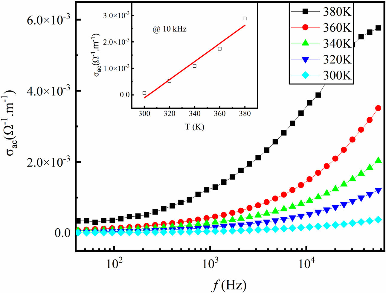
The AC conductivity (σAC) can be obtained by using the formula σAC = 2πf ε0ε' tanδ. Fig. 5 shows the typical results of variation of σAC with frequency for BTNA04 at different temperatures, and the inset displays typical values of σAC at a fixed frequency f = 10 kHz. The solid line is the linear fit. It is clear that the conductivity behavior of the sample exhibits a semiconductor characteristic, which means the value of σAC increases as the temperature or frequency increases. Based on the jump conduction process, the increase of σAC with the increase of temperature may be due to the thermally activated electron jump between the Nb5+ and Ti4+ ions at the octahedral location and the hole jump between Ti4+ and Al3+ ions in the prepared composite sample. As mentioned above, since conduction occurs through electron jumps between Nb5+ and Ti4+ ions and hole jumps between Ti4+ and Al3+ ions, electrons that traverse the grain boundary through a jumping mechanism will accumulate at this interface owing to their elevated resistivity. Consequently, the resultant space charge polarity leads to an enhancement in the dielectric constant [17, 18]. Nevertheless, the research revealed that resistive grain boundaries exhibit greater efficiency when operating at lower frequencies. The enhancement of σAC may be attributed to the presence of low porosity. Similar results can be obtained for the BTNA06 and BTNA08 samples.
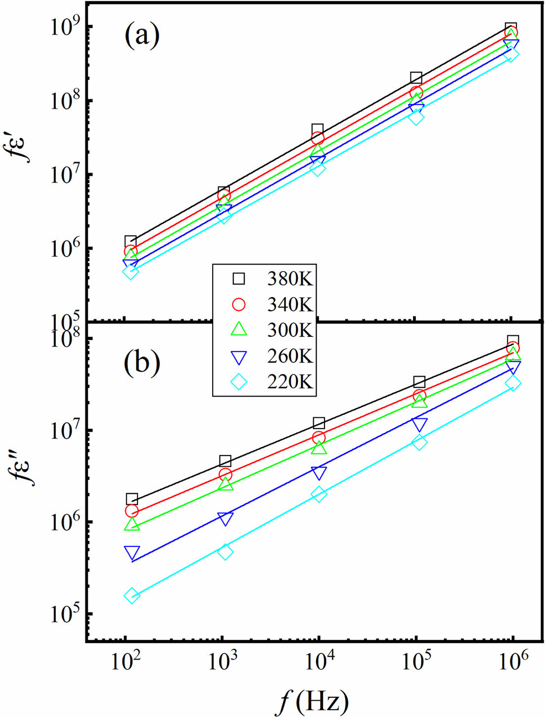
In general, the observed exponential decrease in dielectric loss suggests a correlation between relaxation phenomena and the movement of carrier ions, as well as the corresponding relaxation of neighboring ions. The behavior that was observed can be characterized using a Universal Dielectric Response (UDR) model, as mentioned in reference [19],
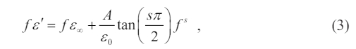
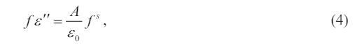
where represents the high-frequency value of e'( f ), e0 denotes the electric permittivity of free space, while A and s are constants.
According to the equations (3) and (4), it is expected that a linear relationship with a slope denoted as s will be observed when plotting log f ε' against log f, as well as log f ε'' against log f, at a specific temperature. The relationship is confirmed in Fig. 6 by a log-log graph for the sample BTNA04. Through the linear fitting, the plot of log ∫ ε' ~log f in Fig. 6(a) yields a value of s about 0.80. Similarly, the plot of log ∫ ε" vs log f in Fig. 6(b) provides a value of s about 0.20-0.36. The obtained values of s are consistent with the UDR model [20]. The parameter s provides insights into the polarizability, complexity, and frequency response characteristics of these perovskite dielectric materials, which can help us understand dielectric characteristics exhibited by these materials and establish a theoretical framework to support their practical utilization.
The phenomena of polarization and dielectric relaxation have a strong correlation with the process of charge transfer. The electrical properties of the internal grains in ceramics exhibit distinct variations when compared to the electrical characteristics observed at the grain borders. Hence, it is imperative to perform an exclusive examination of the internal grains and grain boundaries in order to comprehend the underlying processes of polarization and dielectric relaxation. The electrical characteristics of a ceramic material composed of grains and grain boundaries can be commonly modeled using a series-equivalent circuit with two RC elements [21]. The complex electrical modulus in this particular case can be expressed through the equations [22],
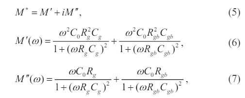
where Rg, Rgb, Cg, and Cgb, are the resistance and capacitance associated with grain and grain boundaries, respectively, and C0 represents the capacitance of a vacuum, and ω =2p f is the angular frequency. At high-frequency limit, equation (6) can be reformulated as
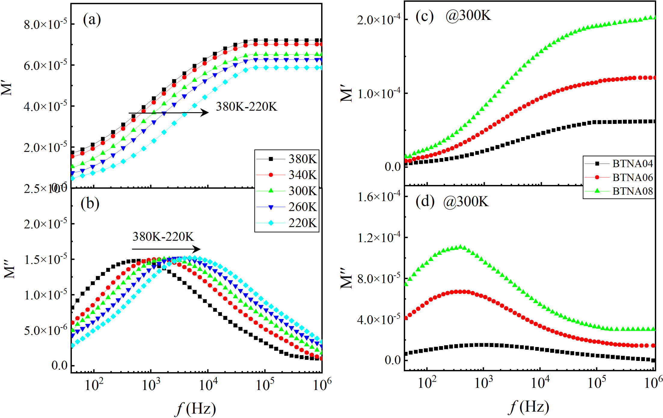
As is known, the electrical resistance and capacitance of grains are significantly lower compared with that of grain boundaries. Thus, the expression M' can be expressed approximately as C0/Cg, indicating that the real component of the modulus in the high frequency region is in inverse ratio to the value of the grain capacitance.
Figures 7(a) and 7(b) show the frequency dependence of M' and M'' for BTNA04 at different temperatures, respectively. It is obvious that the M' plateau in the higher-frequency range increases with temperature increasing. This change indicates the decrease of the capacitance of the grains, as suggested by equation (8). This phenomenon clearly exhibits a quasi-electric dipoles characteristic. This quasi-electric behavior in the high frequency range demonstrates inherent properties within the sample grains, which can be attributed to the influence of ion displacement polarization in the BTNA lattice. When further considering the change of M' and M'' of samples BTNA04, BTNA06, and BTNA08 at 300 K, as shown in Figs. 7(c) and 7(d), it has been observed that the plateau of M' in the high-frequency range exhibits a notable increase as the doping concentration increases. This observation indicates a significant decrease in capacitance and permittivity of the grains with increasing co-doping concentration. With increasing doping content, the resistivity of grains and grain boundaries increased, which led to a decrease in capacitance and permittivity in the measurement frequency range. These results were consistent with the research in Fe-substituted CaCu3Ti4O12 ceramics [23] and Ca+Sr substituted BaTiO3 ceramics [24]. It can be seen that the donor and acceptor co-doping contributes to the temperature and frequency stability of the energy storage properties and the pulsed discharging performance of BaTiO3-based materials, which paved the way of corresponding products into practical application in high-power capacitors [25, 26].
|
Fig. 1 (a) XRD patterns of the prepared samples, (b) The location of the strongest peaks. |
|
Fig. 2 Typical XPS spectra for BTNA04. (a) Ba 3d, (b) Ti 2p, (c) Nb 3d, (d) Al 2p |
|
Fig. 3 Temperature dependence of (a) dielectric constant ε′ and (b) the loss tangent tanδ of BTNA samples at 1 kHz. |
|
Fig. 4 Frequency dependence of (a) dielectric constant ε′ and (b) the loss tangent tanδ of BTNA samples at room temperature. |
|
Fig. 5 Frequency dependence of electrical conductivity of BTNA04 at different temperatures. The inset shows typical values of σac at a fixed frequency f=10 kHz. The solid line is the linear fit. |
|
Fig. 6 Logarithmic plots of frequency dependence of (a) fε' and (b) fε'' for BTNA04 sample at given temperatures. The solid lines are the linear fittings. |
|
Fig. 7 Frequency dependence of the electric modulus (a) M′ and (b) M′′ for BTNA04. Comparison of (c) M′ and (d) M′′ of the samples at 300 K. |
Perovskite-type oxide materials Ba(Al0.5Nb0.5)xTi1-xO3 (x = 0, 0.04, 0.06, 0.08) were prepared using standard solid-state reaction method to investigate the effect of quadrivalent and trivalent elements co-doping on the dielectric and electrical modulus properties. XRD profiles indicate that the Al+Nb co-doping into BaTiO3 does not change the crystal structure significantly with the doping concentration up to 8%. The doping ions exist as Al3+ and Nb5+ chemical state, revealed by the XPS data. The maximum dielectric constant and low dielectric loss were obtained at the doping concentration x = 0.04. The AC conductivity exhibits a semiconductor characteristic as a result of the thermally activated electron jump conduction process. The frequency dependence of the electric modulus implies a quasi-electric dipoles behavior. The results offer valuable insights into the influence of B-site co-doping on the dielectric and electrical modulus properties of BaTiO3-based ceramics and hold relevance for the advancement of new electronic devices. Future research on the temperature and frequency stability of these materials will signify their extended applications in the dielectric and energy storage fields, which is imperative for exploring and developing clean and renewable energy sources.
This work was supported by the National Natural Science Foundation of China (No. 12374031) and the Graduate Innovation Foundation of Yantai University (No. GGIFYTU2315).
- 1. N. Sasirekha and B. Rajesh, Ind. Eng. Chem. Res. 47[6] (2008) 1017-1025.
-

- 2. L. Huang, Z. Chen, J.D. Wilson, S. Banerjee, R.D. Robinson, I.P. Herman, R. Laibowitz, and S. O'Brien, J. Appl. Phys. 100[3] (2006) 1650.
-
- 3. M. Wohlfahrt-Mehrens, J. Schenk, P.M. Wilde, E. Abdelmula, P. Axmann, and J. Garche, J. Power Sources 105[2] (2002) 182-188.
-
- 4. P. Zheng and J.L. Zhang, Acta. Mater. 60[13-14] (2012) 5022-5030.
-
- 5. A. Ioachim, M.I. Toacsan, and M.G. Banciu, J. Eur. Ceram. Soc. 27[2-3] (2007) 1117-1122.
-
- 6. Y. Hiruma, H. Nagata, and T. Takenaka, J. Ceram. Soc. Jpn. 112 (2004) S1125-S1128.
-
- 7. J.G. Park, T.S. Oh, and Y.H. Kim, J. Mater. Sci. 27[21] (1992) 5713-5719.
-
- 8. K.M. Batoo, M. Hadi, and A. Chauhan, Appl. Phys. A-Mater. 128[4] (2022) 1-17.
-
- 9. W.C. Vittayakorn, A. Ruangphanit, and D. Bunjong, J. Adv. Dielectr. 1[2] (2011) 229-235.
-
- 10. H. Dong, W.U. Ying, and M. Ji-Yuan, J. Inorg. Mater. 32[2] (2017) 219.
-
- 11. S.J. Lee, S.M. Park, and Y.H. Han, Jpn. J. Appl. Phys. 48[3] (2009) 031403.
-
- 12. W.Q. Cao, J.W. Xiong, and J.P. Sun, Mater. Chem. Phys. 106[2-3] (2007) 338-342.
-
- 13. L. Ren, M. Zhang, L. Xin, and J. Zhai, Solid State Sci. 131 (2022) 106939.
-
- 14. J.X. Feng, D.S. Hua, and S.T. Xiu, Ferroelectrics 488 (2015) 10-17.
-
- 15. S. Wang, S. Zhang, and X. Zhou, Mater. Lett. 60[7] (2006) 909-911.
-
- 16. X. Zhu, J. Zhu, and S. Zhou, J. Cryst. Growth, 310[2] (2008) 434-441.
-
- 17. S. Kongtaweelert and D.C. Sinclair, Curr. Appl. Phys. 6[3] (2006) 474-477.
-
- 18. I. Soibam, S. Phanjoubam, and H.B. Sharma, Solid State Commun. 148[9-10] (2008) 399-402.
-
- 19. K.M. Hung, W.D. Yang, and C.C. Huang, J. Eur. Ceram. Soc. 23[11] (2003) 1901-1910.
-
- 20. A.K. Jonscher, Nature 267 (1977) 673-679.
-
- 21. N. Bonanos, R.K. Slotwinski, and B.C.H. Steele, J. Mater. Sci. Lett. 3[3] (1984) 245-248.
-
- 22. T.B. Adams, D.C. Sinclair, and A.R. West, Phys. Rev. B 73[9] (2006) 094124.
-
- 23. C. Mu, H. Zhang, Y. He, J. Shen, and P. Liu, J. Phys. D Appl. Phys. 42[17] (2009) 175410.
-
- 24. F.T.Z. Toma, I.N. Esha, Md. Al-Amin, M.N.I. Khan, and K.H. Maria, J. Ceram. Process Res. 18[10] (2017) 701-710.
-
- 25. F. Si, B. Tang, Z. Fang, H. Li, and S. Zhang, J. Alloy Compd. 819 (2020) 153004.
-
- 26. K.J. Lee and W.S. Cho, J. Ceram. Process Res. 13[5] (2012) 527-532.
-
 This Article
-
2024; 25(2): 300-305
Published on Apr 30, 2024
- 10.36410/jcpr.2024.25.2.300
- Received on Feb 21, 2024
- Revised on Mar 16, 2024
- Accepted on Mar 19, 2024
Services
- Abstract
introduction
experimental procedure
results and discussions
conclusion
- Acknowledgements
- References
- Full Text PDF
Shared
Correspondence to
- W.T. Wang
-
School of Physics and Electronic Information, Yantai University, Yantai 264005, P.R. China
Tel : +86-13573512787 Fax: +86-535-6901947 - E-mail: wtwang@ytu.edu.cn
Clean-Energy Research Institute(CRI), Hanyang University, 222, Wangsimni-ro, Seongdong-gu, Seoul, 04763, Korea
E-mail: jcpr@hanyang.ac.kr