- Effect of annealing atmosphere on defects, light absorption and imprinting properties of Bi4Ti3O12 films
Lingxu Wang*, Huiying Liu, Liqiang Liu and Fengqing Zhang*
School of Materials Science and Engineering, Shandong Jianzhu University, Jinan 250101, China
This article is an open access article distributed under the terms of the Creative Commons Attribution Non-Commercial License (http://creativecommons.org/licenses/by-nc/4.0) which permits unrestricted non-commercial use, distribution, and reproduction in any medium, provided the original work is properly cited.
In order to studying the effect of the annealing atmospheres (nitrogen and air) on the films, two kinds of Bi4Ti3O12 (BIT) samples were prepared by the sol-gel and layer-by-layer thermal annealing method. Various factors, including lesser VO••, more V''Bi and greater grain size in the air-annealed samples, interacted on the ferroelectric and light absorption properties. However, more (V''Bi) - (VO••) reinforced the imbalance of electron capture in the ITO/BIT/Au capacitors, resulting in stronger imprinting. And the arrangement of (V''Bi) - (VO••) and the domain pinning in the air-annealed films resulted in more serious aging effect
Keywords: Bi vacancies, Light absorption, Imprinting, Aging
Bismuth-layer perovskite structure ferroelectrics (BLSFs) are mainly applied in high temperature piezoelectric devices and nonvolatile ferroelectric random memories (FeRAM) as a result of their excellent fatigue resistance and high Curie temperature [1-3]. In recent years, BLSFs have also been widely applied in emerging fields such as multiferroic, nanogenerators and optics. Bismuth titanate (Bi4Ti3O12, BIT) is an environment-friendly and promising BLSF material with a Curie temperature of 675 oC [4]. The crystal structure of BIT, belonging to Aurivillius family, consists of a (Bi2O2)2+ fluorite-like layer and a (Bi2Ti3O10)2- perovskite-like block structure staggered along the c-axis [5, 6]. The spontaneous polarization of BIT has obvious anisotropy, and the polarization intensity value along the a-axis and c-axis is ~50 μC/cm2 and ~4 μC/cm2, respectively [7]. In addition, Bi3+ has a special electronic structure [Xe]4f145d106s2 and a pair of 6s2 solitary pair [8]. As a rule, there is a serious deformation in the structure of Bi-containing compounds due to the repulsive force of the special lone pair, resulting in the application of optical properties [9]. Moreover, an internal electric field could be built between (Bi2O2)2+ layer and (Bi2Ti3O10)2- layer, facilitating the separation of photogenic holes and electrons, thus enhancing the photocatalytic and photovoltaic activity [10]. Therefore, it is necessary to study the light absorption performance of BIT.
The effect of preparation technology on the structure and electrical properties of BIT materials is essential. S. K. Badge et al. [4] prepared two kinds of BIT ceramics via sol-gel method and solid state reaction respectively. It was found that the BIT ceramics prepared by sol-gel method had higher crystal density, remanent polarization strength and dielectric constant compared with the sample prepared by solid state reaction method. Chen et al. [11] studied the effect of annealing atmospheres (oxygen, air and vacuum) on the orientation and pro- perties of Bi3.2Pr0.8Ti3O12 (BPTO) films. The BPTO film annealed in oxygen obtained a higher (117) orientation with a lower coercive field strength and a greater remanent polarization. It also possessed no fatigue performance during the switching period of 1011. A. Z. Simões et al. [6] reported that the air-annealed lanthanum-doped bismuth titanate film had higher permittivity than that annealed in oxygen on account of the different grain sizes, crystallinity and structural defects. Hou et al. [12] annealed Bi3.15Nd0.85Ti3O12 (BNT) thin film in nitrogen at 650 oC. The samples had good crystallinity and ferroelectric properties with the remanent polarization (2Pr) of 63.6 μC/cm2 without fatigue. The air- and oxygen-annealed BNT films did not show good performances until annealed at 710 oC and 730 oC respectively. There are few reports about annealing atmosphere effect on the optical, imprinting and aging properties of BIT-based films.
To explore the mechanisms of the annealing atmosphere effect on the properties of the BIT films such as aging, imprinting and light absorption, we prepared the BIT films by sol-gel and annealing in air and nitrogen respectively. The effect of annealing atmosphere on crystal structure and charge defects of the BIT films are discussed in detail.
According to the stoichiometric ratio of Bi4Ti3O12, the preparation of polymeric pecursor solution was completed via the sol-gel method with acetylacetone as chelating agent, ethylene glycol (C2H6O2) as solvent, bismuth nitrate (BiN3O9·5H2O) and tetrabutyl titanate (C16H36O4Ti) as raw materials. Because bismuth salt was volatile at high temperature, it was in excess of 5%. The wet films were obtained by homogenizing on ITO glass substrates with a KW-4A table homogenizer. The wet films were dried at 200 oC and the amorphous dry films were formed by a heating plate of stainless steel. Two batches of the amorphous films were annealed in air and nitrogen respectively under the same annealing process, including heat preservation for 300 s at the annealing temperature of 575 oC. The monolayer poly- crystalline BIT films were obtained. Then the homo- genization and heat treatment process were repeated until the films were about 1 μm. Then two BIT film samples without top electrode were tested for the optical properties. And a layer of dotted Au electrode was sputtered on the surface of the films to form the Au/BIT/ITO capacitors for subsequent tests. In order to obtain the aging BIT films quickly, the films were put into the oven at 60 oC for thermal aging treatment for 60 h.
A Panalytical X'Pert Pro X-ray diffraction (XRD) was used for analyzing the sample structures. The surface and section morphologies of the samples were observed by a Hitachi-Su8010 field emission scanning electron microscope (FESEM). And a radiant precision workstation RT66 was used for testing the hysteresis loops and aging effect of the samples at room tem- perature. A TH2828S automatic component analyzer was applied in testing the dielectric performances. And the valence state of the elements and the state of the charged defects of the films were analyzed by a Wscabb X-ray photoelectron spectrometer. The UV-VIS diffuse reflectance spectrums were tested via a Hitachi U-4100 spectrophotometer.
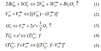
Previous research results show that the change of defect state is one of the main factors affecting the structure and various electrical performances of ferroelectric films [13-15]. Additionally, even a small number of surface defects have great potential in adjusting band structure and carrier concentration [16]. The formation of the possible point defects and defect dipoles in the BIT film are summarized. Firstly, the bismuth vacancies (V''Bi) are formed due to the inevitable bismuth volatilization in the process of film preparation, and the oxygen vacancies (VO••) are generated nearby to maintain charge neutrality [Eq. (1)]. And the defect dipoles (V''Bi) - (VO••) may be formed [Eq. (2)]. Secondly, previous research [13, 17] shows that annealing in nitrogen promoted the oxygen atom overflow, which resulted in more oxygen vacancies in ferroelectric film materials [Eq. (3)]. In addition, if the Ti atoms in the lattice capture the electrons presented in Eq. (3), the valence of Ti atoms will be changed, so the negatively charged ions (Ti3+Ti4+) are formed [Eq.(4)]. The corresponding defect dipoles (Ti3+Ti4+)' - VO•• also be formed by (Ti3+Ti4+)' and VO•• [Eq.(5)].
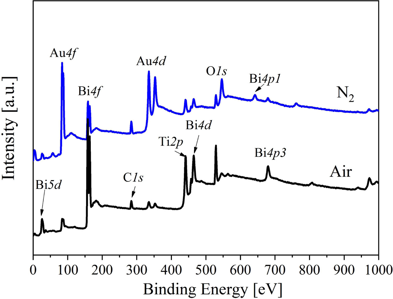
For understanding the element valence state and defect state of the BIT films annealed in different atmospheres, XPS test and analysis are accomplished on the sample surfaces. The XPS wide sweep spectrum of the two samples as shown in Fig. 1. Except for C1s, Au4f and Au4d orbital peaks are also detected due to the Au top electrode sputtered on the surface of the BIT films.
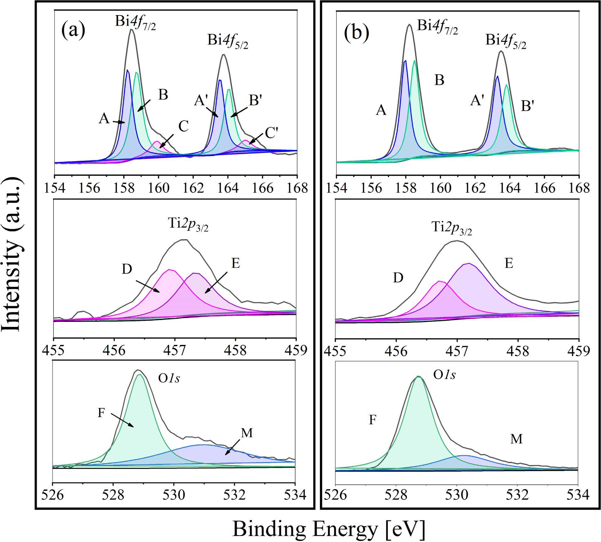
In addition, the Lorentz-gauss formula is applied in fitting the XPS peaks of Bi4f, Ti2p3/2 and O1s respectively. Because of the superposition of partial peaks of Ti2p1/2 and Bi4d3/2, Ti2p3/2 is chosen instead of Ti2p to be fitted. And the two kind of BIT film samples show significant differences in the peak seg- mentation in Fig. 2. In Fig. 2(a), the main peak position of Bi4f7/2 (158.5 eV) and Bi4f5/2 (163.8 eV) in the samples annealed in nitrogen is typical Bi4f spin orbit dipole splitting energy based on the formula D(Bi4f5/2 - Bi4f7/2) = 5.3 eV. The peak group including A (158.2 eV) and A' (163.5 eV) is the result of the production of bismuth suboxide [18], besides the peak group of B (158.5 eV) and B' (163.8 eV) could be regarded as the main contribution of Bi3+ cation in the lattice [19]. There is also a group of spin orbit dipole C (159.9 eV) and C' (165 eV), which can be classified as Bi metal (Bi0) according to the literature [17]. The reason for the occurrence of Bi0 is inferred as the exposure to reduction atmosphere during the annealing process. Accordingly, as shown in Fig. 2(b), there is no peak group of C and C' in the Bi4f orbital fitting peaks of the air-annealed film sample. In addition, the shift of Ti2p3/2 peak to low binding energy reveals the transition of Ti from Ti4+ to Ti3+ [20]. The component peak D represents Ti3+, while the component peak E represents Ti4+. According to the fitting results, Ti3+:Ti4+ area ratio of the nitrogen and air-annealed films is 1:0.89 and 1:1.88, respectively, indicating that the samples annealed in nitrogen contained more Ti3+. Based on the XPS information of O1s orbital, the component peak F around 528.8 eV corresponds to lattice oxygen, besides the component peak M with higher binding energy corresponds to oxygen vacancy or adsorption oxygen [21]. Similarly, the proportion of the lattice oxygen in two samples can be obtained by calculating the fitting area. The proportion of the lattice oxygen in the nitrogen annealing sample is 57%, while that in the air annealing sample is 76%. It indicates that more VO•• are produced in the nitrogen annealed sample.
Through analyzing above-mentioned aspects, after eliminating the influence of Bi0, oxygen outside the lattice and other factors, the fitting area of Bi4f,Ti2p3/2 and O1s orbits and the corresponding sensitivity factors of each element are used for the quantitative study of XPS, so as to determine the distribution of surface atoms. About BLSF material, the formation energy of cation vacancy is similar to that of anion vacancy, while the binding energy of Ti vacancy is very higher, so Ti atoms are relatively stable in the lattice [22]. Therefore, the approximate ratio of surface atoms is calculated based on Ti represented by Ti2p3/2. After calculation, the approximate Bi/Ti/O ratios of the BIT film samples annealed in nitrogen and air are 2:1:5.3 and 1.4:1:5.3, respectively, indicating that the annealing atmospheres have a certain effect on the stoichiometric ratio of Bi4Ti3O12. In addition, the concentration of Bi ions in the lattice of the air-annealed samples is significantly lower than that of the nitrogen-annealed samples. It is deduced that the air-annealed sample might contain a higher concentration of the bismuth vacancies (V''Bi). Xu et al. also found that in BiFeO3 annealed in a higher oxygen partial pressure atmosphere, the defect formation energy of the V''Bi was lower than that of the VO•• [23].
Summing up the above, there are more V''Bi in the air-annealed samples with certain resulting VO••, while there are more VO•• due to the valence change of Ti from Ti4+ to Ti3+ in the nitrogen-annealed samples. In addition, (V''Bi) - (VO••) is the main defect dipole in the air-annealed samples, while (Ti3+Ti4+') - (VO••) is the main defect dipole in the nitrogen-annealed samples.
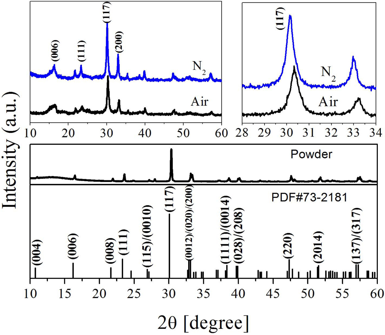
The XRD spectrum of the BIT film samples annealed in different atmospheres are drawn, as Fig. 3. The spectras of the Bi4Ti3O12 powder and the standard PDF card (JCPDS 73-2181) are also showed for comparison. It is observed that all the films are monophasically, and no obvious impurity peaks (including Bi0) is detected. The diffraction peaks of the samples in accordance with those of the orthogonal Fmmm space group. Eq. (6) can be applied in calculating the grain orientation of the film samples [24]:
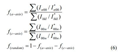
Where Ihkl is the tested intensity of the diffraction peak (hkl) of the film sample and I*hkl is the corres- ponding peak (hkl) strength of the Bi4Ti3O12 powder. The calculated results are listed in Table 1. The grains of a-axis and c-axis orientation are lesser in the sample whether it is prepared in air or nitrogen, indicating that the films are dominated by random orientation [25]. It indicates that there is a little influence of the annealing atmospheres on the grain orientation of the prepared BIT films. The average grain size of the BIT films are obtained via using the Scherrer formula. The average grain size of the air-annealed samples is about 19.1nm, and that of the nitrogen-annealed samples is about 25.6nm. Obviously, the samples annealed in nitrogen show better grain development and larger grain size. As the magnification of 2θ from 28o to 34o, the XRD pattern of the air-annealed samples shows obvious displacement in the direction of large angle. It may be due to the more generation of V''Bi, the decrease of the number of atoms in the crystal and the coulomb force between atoms, resulting in a decrease of cell volume [26, 27].
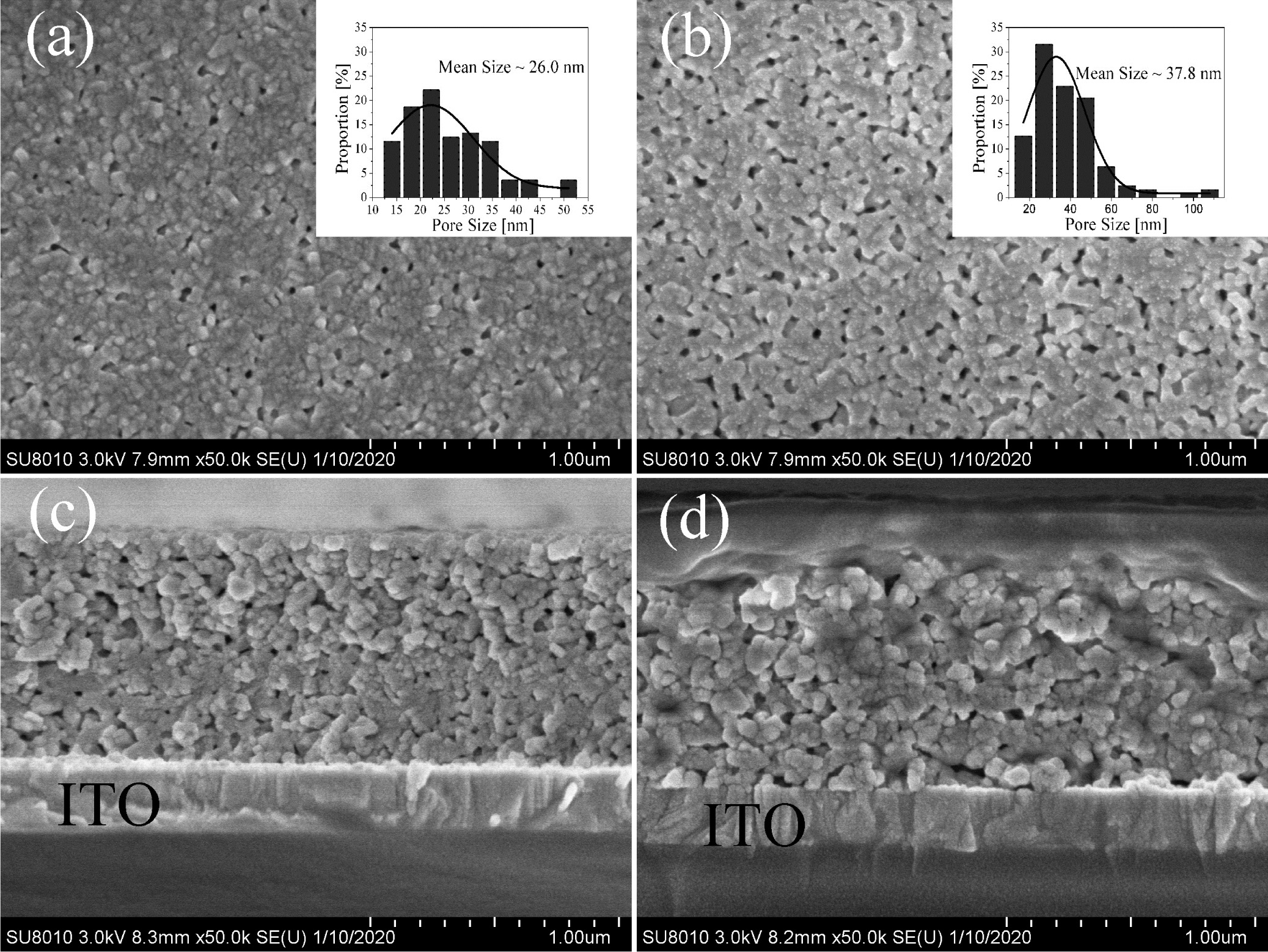
Fig. 4 shows FE-SEM morphologies of the surface and section of the BIT film samples annealed in different atmospheres. The surface of the films are relatively smooth, uniform and free of large cracks. However, due to the volatilization of the organic compounds and Bi element during the annealing process, the micropore defects appear inevitably. From Fig. 4(a), the surface of nitrogen-annealed sample shows obvious grains and grain boundaries, while the smaller grains in the air-annealed sample (Fig. 4(b)) aggregate into blocks without crystal boundaries. It is consistent with the average grain size result of the samples analyzed via XRD test. Nano Measurer software is used for fitting the average size of surface micropores of the samples, as shown in the embedded figure of Fig. 4(a) and (b). Obviously, compared with the air-annealed samples with an average micropore size of 37.8 nm, the nitrogen-annealed sample with an average micropore size of 26.0 nm have smaller porosity. In summary, the different annealing atmospheres have a certain effect on the surface morphology of the BIT film samples. The reasons for this phenomenon may be as follows: (1) The nucleation rate of the film is higher when annealed in a higher oxygen partial pressure atmosphere, resulting in the reduction of grain size [6]. (2) The excess VO•• promote grain growth by promoting mass transfer between reactants in reductive atmospheres or hypoxia conditions [28]. Besides, it can be found from Fig. 4(c) and (d) that the BIT films obtained by annealing in two different atmospheres have obvious boundaries with the ITO glass substrates, and the thicknesses are all around 1μm.
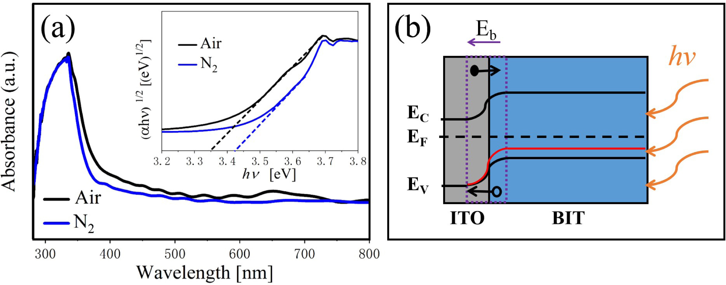
The optical property of the samples are investigated using the UV-VIS diffuse reflection spectrum in the wavelength range of 250~800 nm. From Fig. 5(a), the air-annealed BIT films have stronger absorption in the λ = 300~500 nm region. The optical band gap values of the samples are calculated using Eq. (7) [29]:

Where, α is a constant, h is the Planck constant, A is the absorption coefficient near the absorption edge, Eg is the absorption band gap energy, and for BIT with indirect band gap, n = 4 [30]. The inset diagram shows (ahv)1/2 vs.(hv)relationship near the absorption edge of the films, and the bandgap values are given by the epitaxy of the linear regions. The band gap value of the air and nitrogen annealed samples are 3.35 eV and 3.47 eV, respectively. It can be seen that the air-annealed samples possess better light absorption capacity compared with the nitrogen-annealed samples. The possible reasons are as follows: (1) The smaller grain size [31, 32]. More reaction and light absorption site are provided by the larger specific surface area of the air-annealed samples, which will increase the effective area of light absorption, thus promoting the transition of photoexcited carriers. (2) The smaller concentration of the oxygen vacancies [33]. The oxygen vacancies are considered to be the main cause of trapping and composite the charge carriers, which can lead to the degradation of the photovoltaic performance of the ferroelectric materials with bandgap engineering. (3) The larger concentration of the bismuth vacancies on the surface [16]. The higher concentration of V''Bi on the surface of the air-annealed samples could adjust the electronic structure greatly and establish a new defect energy level in the forbidden zone. The possible energy band diagram of the BIT films annealed in different atmospheres in the test process of UV-VIS diffuse reflectance are shown in Fig. 5(b). Bi4Ti3O12 are considered to be a p-type semiconductor with a work function greater than 6.1 eV [34]. The holes have an advantage over oxygen ions in conducting electricity at room temperature [35]. Since the work function of ITO substrate (4.85 eV) is smaller than that of BIT, there will be a downward band bend and a schottky barrier field Eb in the depletion area of ITO/BIT interface, thus promoting the separation of photoexcited electron-hole pairs and generating photocurrent [36]. The defect energy level (red line in the figure) established in the forbidden band due to more V''Bi in the air-annealed samples is beneficial to the transition of electrons towards the conduction band under irradiation, which makes the carrier concentration and electron conductivity higher. And the electric field Eb increases, thereby facilitating charge separation.
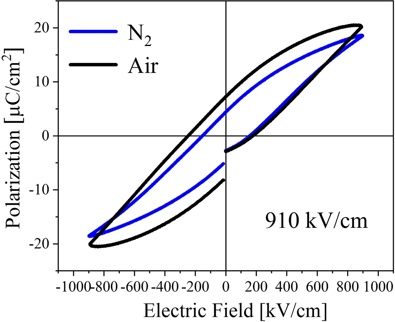
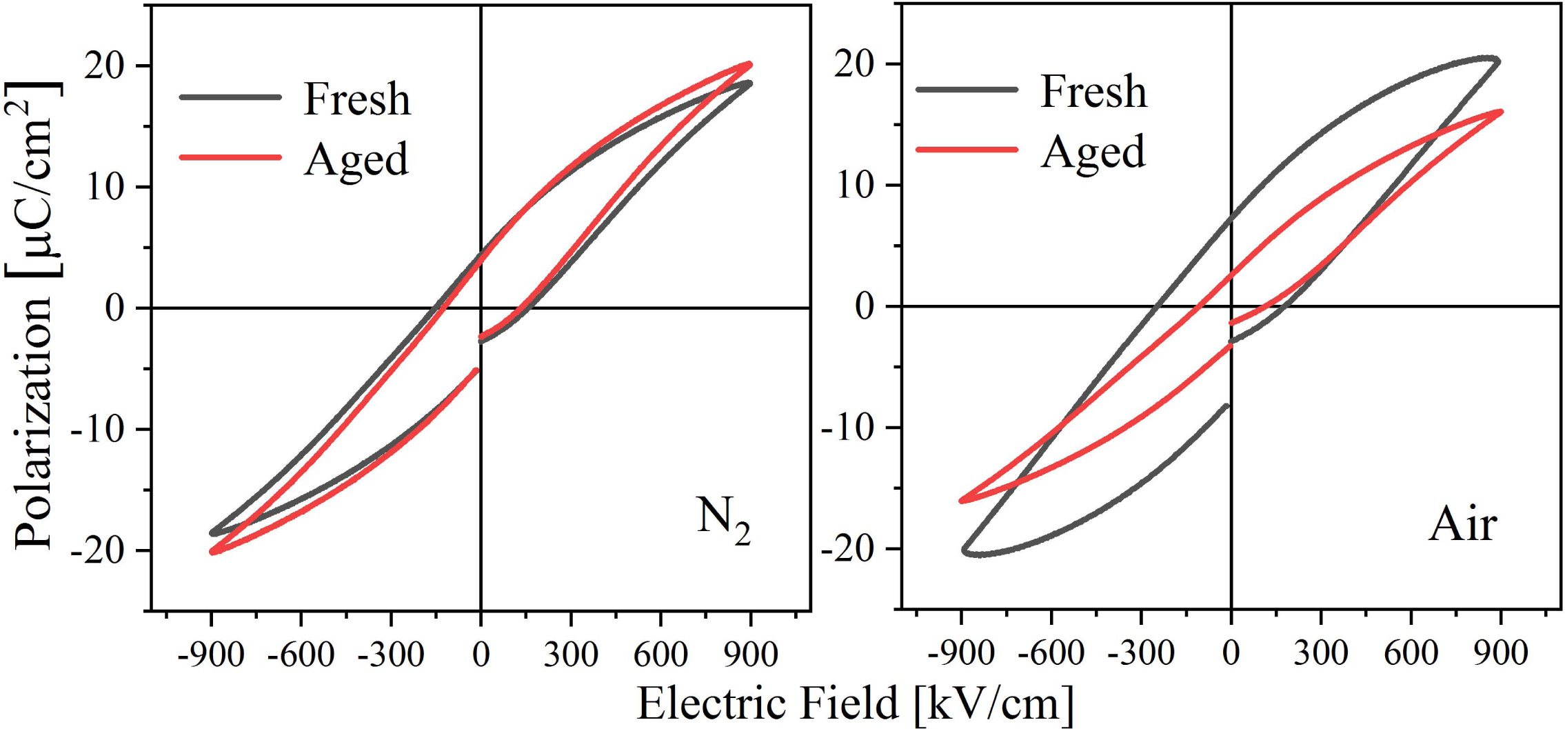
Fig. 6 shows the ferroelectric performance of the BIT films prepared in different atmospheres, and the test electric field is 910 kV/cm. Annealed in nitrogen and air, the remanent polarization strength (2Pr) of the samples are 9.6 μC/cm2 and 15 μC/cm2, and the coercive field strengths are 309.8 kV/cm and 424.5 kV/cm, respectively. Interestingly, the air-annealed samples have higher remanent polarization strength and stronger coercive field compared with annealing in nitrogen. It is evident that the ferroelectric performance is affected by the competitive mechanism of various factors. The larger remanent polarization may be due to: (1) The larger lattice distortion of the air-annealed samples increases the degree of polarization [26]. (2) There are more free V''Bi in the air-annealed samples, which could promote the ferroelectric domain migration and improve the ferroelectric performance [6]. (3) There are few VO•• in the air-annealed samples. The accumulation of VO•• in the domain boundaries could cause domain pinning, thus hindering the polarization switching. Additionally, the stronger coercive field may be due to: (1) The average grain boundary area (the area where the domain walls may be pinned by the defect dipoles) of the small grains in the air-annealed samples is larger than the large grains in the nitrogen-annealed samples, so the probability of the domain walls of the air-annealed samples to be pinned is higher [37]. (2) It may be related to the different amplitude of polarization, the way of domain growth, and the concentration ratio between the domain walls and grain boundaries in the films [38].
In addition, it can be seen from Fig. 6 that the imprinting effect appears. The hysteresis loop of the air-annealed films appears obvious deviation along the negative direction of the electric field axial, which results from the internal electric field (Ei). The Ei can be defined as:

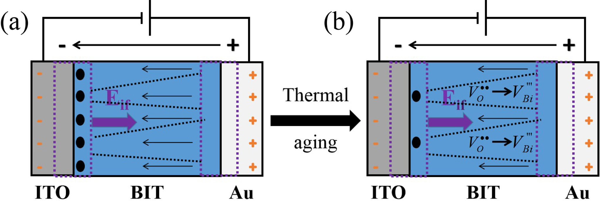
Where +EC (-EC) is the positive (negative) coercive field strength. The Ei of the nitrogen- and air-annealed samples are calculated to be 2.0 kV/cm and -34.72 kV/cm, respectively. The hysteresis loop of the air-annealed BIT films shows an obvious negative voltage deviation, indicating that an internal electric field Eif pointing to the top electrode is created by the electron capture mechanism at the bottom electrode interface [28, 39]. The work function of Au is 5.1 eV and that of ITO is 4.85 eV, so two schottky barriers with different barrier heights are formed in ITO/BIT and BIT/Au interfaces [40]. A net built-in electric field Eif, from the higher barrier to the lower barrier, could be generated by the asymmetric schottky barriers between the two interfaces in the BIT film [34], as shown in Fig. 7(a). Therefore, more VO•• could accumulate in the bottom ITO/BIT interface than in the top BIT/Au interface, resulting in the generation of more (V''Bi) - (VO••) and forming a defect layer [41, 42].
The net polarization, determining the electron capture location, contains two parts: PP (the ferroelectric per- ovskite polarization) and PD (the volume distribution of the defect dipole complexes) [43]. The work function of the ITO conductive glass (4.85 eV) is lower than that of Au (5.1 eV) [44]. In consequence, more oxygen vacancies will accumulate at the BIT/ITO bottom interface than at the Au/BIT top interface with the cycles of switching polarization in the Au/BIT/ITO ferroelectric film capacitors, resulting in more defect dipoles (V''Bi) - (VO••) [45, 46]. Correspondingly, a stronger PD appears on the BIT/ITO interface. Through research, W. L. Warren et al. [39] found that intensive net polarization at an electrode interface could result in enhanced electron capture. Therefore, the asymmetric distribution of the trapped electrons in the interface between the ferroelectric film and the top and bottom electrode would lead to imprinting. Song et al. [47] believed that the ferroelectric performance of the Aurivillius BIT films are actually affected by the defect dipole com- plexes (V''Bi) - (VO••) rather than VO•• or V''Bi. The (V''Bi) - (VO••) complexes are easily formed in the air-annealed samples. Moreover, researchers such as W. L. Warren also deem that the cation vacancies (V''Bi) may be the additional electron capture locations. Thus, there is a larger Eif in the air-annealed BIT film. Similarly, A.Z. Simões et al.[6] found that the hysteresis loop of the lanthanum-doped oxygen-annealed BIT film was signi- ficantly deviated along the positive direction of the electric field axis, which was due to the high concen- tration of the V''Bi and VO•• in the film/electrode interface. Therefore, the asymmetric polarization switching that resulted in the imprinting is caused by the asymmetric distribution of the captured electrons at the top and bottom interface of the Au/BIT/ITO capacitor, which is aggravated by more (V''Bi) - (VO••) and V''Bi in the air-annealed sample.
Since the properties of the prepared BIT films are relatively stable, they are put into an oven at 60 oC for thermal aging treatment for 60 h in order to obtain the aged samples as soon as possible for research. The comparison of the hysteresis loops of the samples before and after aging is shown in Fig. 8. After aging treatment, the 2Pr of the nitrogen-annealed sample decreased by 5.6%, while the 2Pr of the air-annealed sample decreased by 62.3%. It can be seen that the air-annealed aging sample presents significant degradation of the ferroelectric properties. It is generally assumed that the aging of the ferroelectric films results from the gradual fixation of the local domain structures and domain walls over time, which prevents the domain structures from switching with the applied electric field [48]. After thermal aging treatment, the VO•• in the BIT films that are easy to move will not only transition over a short distance, but also lead to a long distance migra- tion. The short-distance VO•• transition rearranges or reorientates the defect dipoles (V''Bi) - (VO••) in the volume and stabilizes the domain structure, a mechanism known as the volume effect [49]. However, the long-distance VO•• migration to the interfaces such as grain boundaries can realize the pinning of the domain walls to prevent the switching of domain (grain boundary effect) [50]. Therefore, the aging of the air-annealed sample with larger average grain boundary area and more (V''Bi) - (VO••) dipoles is more serious. In addition, it is found that the imprinting effect of the air-annealed aging sample disappears, because the captured charge tended to relax in the thermal aging process [48].
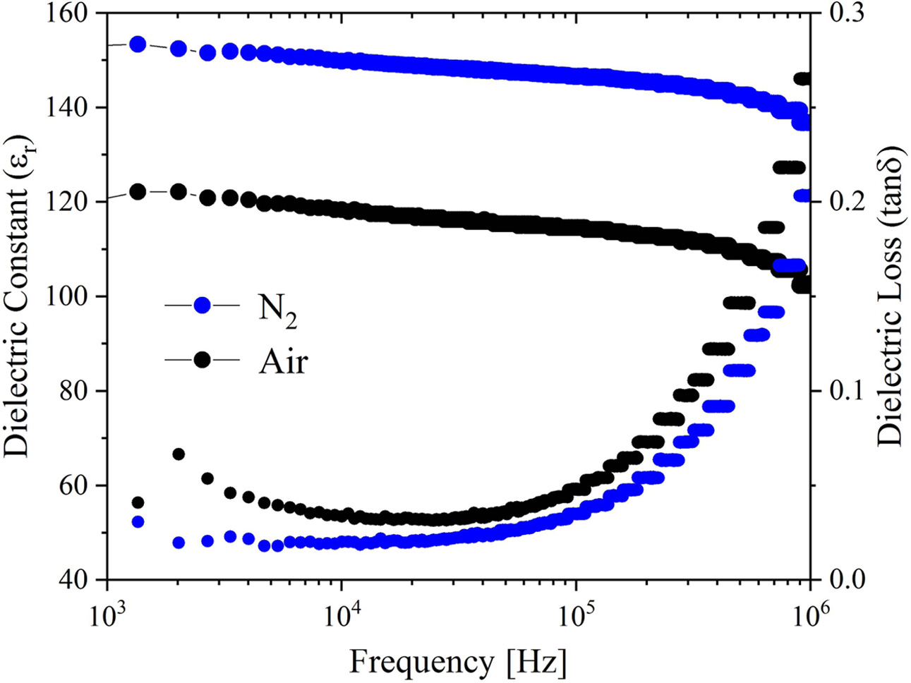
As shown in Fig. 9, the dielectric constant (εr) and dielectric loss (tanδ) of the BIT ferroelectric films vary with the test frequency. The εr of the two samples have good frequency stability in the frequency range of 103~106 Hz. The dielectric losses increase with the frequency increase, which can be mainly derived from that the tanδ is dominated by the leakage current at low frequency and the inertia of the electric dipoles at frequency higher than 104 Hz [28]. At 104 Hz, the εr of the samples annealed in air and nitrogen are 118.3 and 149.7, respectively, and the dielectric losses are 0.03 and 0.02, respectively. The good dielectric performance of the nitrogen-annealed sample is mainly due to the larger grain size, better crystallinity and fewer structural defects (micropores) [6, 51]. It is speculated that the larger porosity on the surface of the air-annealed samples affects the interface polarization, resulting in the decrease of dielectric constant [38].
|
Fig. 1 XPS wide sweep spectrum of the BIT films annealed in different atmospheres. |
|
Fig. 2 XPS narrow sweep spectra of Bi, Ti, O elements in the BIT films annealed in different atmospheres: (a) nitrogen, (b) air. |
|
Fig. 3 XRD patterns of the BIT films annealed in different atmospheres. |
|
Fig. 4 FE-SEM surface and section morphologies of the BIT films annealed in different atmospheres: (a) & (c) nitrogen, (b) & (d) air. |
|
Fig. 5 UV-VIS absorption spectrum and energy band diagram of the BIT films annealed in different atmospheres. |
|
Fig. 6 Hysteresis loops of the BIT films annealed in different atmospheres. |
|
Fig. 7 Imprinting (a) and aging (b) schematic diagrams of the BIT films annealed in different atmospheres. |
|
Fig. 8 Diagram of hysteresis loops of the BIT films annealed in different atmospheres before and after thermal aging process. |
|
Fig. 9 Relation curves of dielectric constant, dielectric loss and frequency of the BIT films annealed in different atmospheres. |
|
Table 1 Crystal structure data of the BIT films annealed in different atmospheres |

The Bi4Ti3O12 films were prepared by the sol-gel and layer-by-layer thermal annealing method. The annealing atmosphere (nitrogen, air) effect on the growth and properties of the films were studied. The smaller average grain size and the greater average micropore size of the air-annealed samples were found through XRD and FE-SEM analysis. And according to XPS analysis, the air-annealed samples had lesser VO•• and more V''Bi. Under the combined action between the effect of the crystal structure and charged defect, the air-annealed sample had a relatively narrow band gap of 3.35eV, a relatively larger remanent polarization intensity (2Pr = 15 μC/cm2) and a stronger coercive field (2EC = 424.5 kV/cm). More defect dipoles (V''Bi) - (VO••) in the defect layer at the ITO/BIT interface reinforced the imbalance of electron capture in the ITO/BIT/Au capacitors, resulting in more serious imprinting. The arrangement of the defect dipoles (V''Bi) - (VO••) and the domain pining in the air-annealed films resulted in the stronger aging effect.
This work was supported by funding from the Research Fund for the Doctoral Program of Shandong Jianzhu University (Grant No. XNBS1626) and the Program of the Housing and Urban-Rural Construction Department of Shandong Province (2019-K7-10).
- 1. F.Q. Zhang, O. Wahyudi, Z.H. Liu, H. Gu, and Y.X. Li. J. Alloy. Compd. 753 (2018) 54-59.
-

- 2. C.H. Jia, Y.H. Chen, L.H. Ding, and W.F. Zhang, Appl. Surf. Sci. 253 (2007) 9506-9512.
-

- 3. J.Y. Chen, Q. Yun, W. Gao, Y.L. Bai, C.H. Nie, and S.F. Zhao, Mater. Lett. 136 (2014) 11-14.
-

- 4. S.K. Badge, and A.V. Deshpande, Solid State Ionics 334 (2019) 21-28.
-

- 5. G. Parida, and J. Beran, Ceram. Int. 40 (2014) 3139-3144.
-

- 6. A.Z. Simões, A. Ries, B.D. Stojanovic, G. Biasotto, E. Longo, and J.A. Varela, Ceram. Int. 33 (2007) 1535-1541.
-

- 7. S.E. Cummins, and L.E. Cross, J. Appl. Phys. 39 (1968) 2268.
-

- 8. D.G. Gu, Y.Y. Qin, Y.C. Wen, T. Li, L. Qin, and H.J. Seo, J. Alloy. Compd. 695 (2017) 2224-2231.
-

- 9. S. Amano, and H. Yamane, J. Alloy. Compd. 675 (2016) 377-380.
-

- 10. Y. Liu, M.Y. Zhang, L. Li and X.T. Zhang, Appl. Catal. B-Environ. 160-161 (2014) 757-766.
-

- 11. H.Z. Chen, M.C. Kao, S.L. Young, C.C. Yu, C.H. Lin, C.M. Lee, and C.R. Ou, Thin Solid Films 517 (2009) 4818-4821.
-

- 12. F. Hou, M.R. Shena, and W.W. Cao, Thin Solid Films 471 (2005) 35-39.
-

- 13. F.Q. Zhang, P. Shen, H.Y. Liu, L.X. Wang, X.D. Guo, X.F. Zhao, Z.B. Ma, Q.B. Tian, and S.H. Fan, Ceram. Int. 46 (2020) 4314-4321.
-

- 14. X.F. Zhao, H.Y. Liu, X.Y. Pan, L.X. Wang, Z. Feng, X.D. Guo, P. Shen, Z.B. Ma, F.Q. Zhang, Q.B. Tian, and S.H. Fan, Ceram. Int. 46 (2020) 10536-10544.
-

- 15. Z.T. Li, H. Liu, H.C. Thong, Z. Xu, M.H. Zhang, J. Yin, J.F. Li, K. Wang, and J. Chen, Adv. Electron. Mater. 2018, 1800756.
-

- 16. J. Di, C. Chen, C. Zhu, M.X. Ji, J.X. Xia, C. Yan, W. Hao, S.Z. Li, H.M. Li, and Z. Liu, Appl. Catal. B-Environ. 238 (2018) 119-125.
-

- 17. H.Y. Liu, L.X. Wang, F.Q. Zhang, X.D. Guo, P. Shen, X.F. Zhao, and S.H. Fan, Ceram. Int. 45 (2019) 18320-18326.
-

- 18. S.R. Sainkar, S. Badrinarayan, and A. Goswami, J. Electron. Spectrosc. 25 (1982) 181-189.
-

- 19. M.W. Chu, M. Ganne, M.T. Caldes, and L. Brohan, J. Appl. Phys. 91 (2002) 3178-3187.
-

- 20. D. Chen, H.T. Zhang, R.K. Chen, X.Y. Deng, J.B. Li, G.Q. Zhang, and L.M. Wang, Phys. Status Solidi A 209 (2012) 714-717.
-

- 21. Y. Li, X.X. Cui, N.N. Sun, J.H. Du, X.W. Li, G.X. Jia, and X.H. Hao, Adv. Optical Mater. 7 (2018) 1801105.
-

- 22. P. Ctibor, J. Čížek, J. Sedláček, and F. Lukáč, J. Am. Ceram. Soc. 100 (2017) 2972-2983.
-

- 23. Q. Xu, M. Sobhan, Q. Yang, F. Anariba, K.P. Ong, and P. Wu, R. Soc. Chem. 43 (2014) 10787-10793.
-

- 24. S.A. Ma, X.W. Cheng, T. Alia, Z.L. Ma, Z.J. Xu, and R.Q. Chu, Appl. Surf. Sci. 463 (2019) 1141-1147.
-

- 25. J. Li, J. Yu, G. Peng, Y.B. Wang, and W.L. Zhou, J. Am. Ceram. Soc. 90 (2007) 3220-3223.
-

- 26. Q. Chen, F. Gao, J. Xu, C.Y. Wu, S.Y. Cao, Y.T. Guo, E. Pawlikowska, M. Szafran, and G.H. Cheng, J. Am. Ceram. Soc. 103 (2020) 1912-1926.
-

- 27. J. Li, N. Sha, and Z. Zhao, Appl. Surf. Sci. 454 (2018) 233-238.
-

- 28. C. Feng, C.H. Yang, F.J. Geng, P.P. Lv, and Q. Yao, J. Eur. Ceram. Soc. 36 (2016) 527-532.
-

- 29. H.P. Zhang, M.K. Lü, S.W. Liu, L.Y. Wang, Z.L. Xiu, Y.Y. Zhou, Z.F. Qiu, A.Y. Zhang, and Q. Ma, Mater. Chem. Phys. 114 (2009) 716-721.
-

- 30. Z.W. Chen, H. Jiang, Wu. L. Jin, and C.K. Shi, Appl. Catal. B-Environ. 180 (2016) 698-706.
-

- 31. W.F. Yao, H. Wang, X.H. Xu, J.T. Zhou, X.N. Yang, Y. Zhang, and S.X. Shang, Appl. Catal. A-Gen. 259 (2004) 29-33.
-

- 32. M. Li, H.J. Sun, X.F. Liu, H.T. Sui, and P.D. Liu, Mater. Lett. 219 (2018) 4-7.
-

- 33. H.Y. Xiao, Y.F. Wang, N. Jiao, Y.P. Guo, W. Dong, H. Zhou, Q. Li, and C.J. Sun, Adv. Electron. Mater. 5 (2019) 1900407.
-

- 34. H.C. He, Z.L. He, Z. L. Jiang, J. Wang, T. Liu, and N. Wang, J. Alloy. Compd. 694 (2017) 998-1003.
-

- 35. Y. Chen, S.X. Xie, H.M. Wang, Q. Chen, Q.Y. Wang, J.G. Zhu, and Z.W. Guan, J. Alloy. Compd. 696 (2017) 746-753.
-

- 36. K. Wang, H.W. Zheng, X.J. Li, G.L. Yuan, W.X. Gao, L. Wei, X.A. Zhang, and W.F. Zhang, Mater. Lett. 179 (2016) 182-185.
-

- 37. J.P. Cruz, E. Joanni, P.M. Vilarinho, and A.L. Kholkin, J. Appl. Phys. 108 (2010) 114106.
-

- 38. T. Pandirengan, M. Arumugam, and M. Durairaj, Thin Solid Films 628 (2017) 117-126.
-

- 39. W.L. Warren, D. Dimos, G.E. Pike, B.A. Tuttle, and M.V. Raymond, R. Ramesh, J.T. Evans Jr., Appl. Phys. Lett. 67 (1995) 866.
-

- 40. Y. Zhou, C. Wang, S.L. Tian, X.K. Yao, C. Ge, E.J. Guo, M. He, G.Z. Yang, and K.J. Jin, Thin Solid Films, 698 (2020) 137851.
-

- 41. B.C. Jeon, D. Lee, M.H. Lee, S.M. Yang, S.C. Chae, T.K. Song, S.D. Bu, J.S. Chung, and T.W. Noh, Adv. Mater. 25 (2013) 5643-5649.
-

- 42. Y.J. Zhang, H.W. Zheng, X.W. Wang, H. Li, Y.H. Wu, Y.Z. Zhang, H.X. Su, and G.L. Yuan, Ceram. Int. 46 (2020) 10083-10088.
-

- 43. G.E. Pike, W.L. Warren, D. Dimos, B.A. Tuttle, and R. Ramesh, J. Lee, V.G. Keramidas, and J.T. Evans, Appl. Phys. Lett. 66 (1995) 484.
-

- 44. B.H. Park, T.W. Noh, J. Lee, C.Y. Kim, and W. Jo, Appl. Phys. Lett. 70 (1997) 1101.
-

- 45. H.C. Thong, Q. Li, M.H. Zhang, C.L. Zhao, K.X. Huang, J.F. Li, and K. Wang, J. Am. Ceram. Soc. 101 (2018) 3393-3401.
-

- 46. W.G. Liu, J. Ko, and W.G. Zhu, Mater. Lett. 49 (2001) 122-126.
-

- 47. D.P. Song, X.W. Tang, B. Yuan, X.Z. Zuo, J. Yang, L. Chen, W.H. Song, X.B. Zhu, and Y.P. Sun, J. Am. Ceram. Soc. 97 (2014) 3857-3863.
-

- 48. B. Akkopru-Akgun, W.L. Zhu, M.T. Lanagan, and S. Trolier-McKinstry, J. Am. Ceram. Soc. 102 (2019) 5328-5341.
-

- 49. K. Yan, F.F. Wang, D.W. Wu, X.B. Ren, and K.J. Zhu, J. Am. Ceram. Soc. 102 (2019) 2611-2618.
-

- 50. M.I. Morozov, and D. Damjanovic, J. Appl. Phys. 104 (2008) 034107.
-

- 51. T. Pečnik, S. Glinšek, B. Kmet, and B. Malič, J. Alloy. Compd. 646 (2015) 766-772.
-

 This Article
-
2021; 22(1): 121-129
Published on Feb 28, 2021
- 10.36410/jcpr.2021.22.1.121
- Received on May 18, 2020
- Revised on Jul 26, 2020
- Accepted on Aug 14, 2020
 Services
- Abstract
introduction
experimental process
results and discussion
conclusion
- Acknowledgements
- References
- Full Text PDF
Shared
 Correspondence to
- Lingxu Wang and Fengqing Zhang
-
School of Materials Science and Engineering, Shandong Jianzhu University, Jinan 250101, China
Tel : +86053186367285 Fax: +86053186367285 - E-mail: keji424@126.com


 Copyright 2019 International Orgranization for Ceramic Processing. All rights reserved.