- Refractive-index matched layers applied to flexible conductive MTO/Ag/MTO multilayer films on the PET substrate
Sangmoo Yoon and Guneik Jang*
Department of Materials Engineering, Chungbuk National University
This article is an open access article distributed under the terms of the Creative Commons Attribution Non-Commercial License (http://creativecommons.org/licenses/by-nc/4.0) which permits unrestricted non-commercial use, distribution, and reproduction in any medium, provided the original work is properly cited.
A hybrid structure of Mn (2.59 wt.%) doped SnO2 (MTO)/Ag/MTO films with refractive index matching layers (IMLs) was deposited on PET substrate by a RF/DC magnetron sputtering method at room temperature. To match the refractive index (n) of MTO/Ag/MTO/PET film, high and low refractive index materials of MTO (n = 2.02) and SiO2 (n = 1.52) were placed between MTO/Ag/MTO and PET substrate, respectively. In order to evaluate the effect of IMLs on the reflectivity and color variation, an optical simulation program, Essential Macleod Program (EMP) was adopted, in advance. From EMP simulation, the multilayer film of MTO (40 nm)/Ag (13 nm)/MTO (40 nm) with optimized IMLs of SiO2 (120 nm)/MTO (10 nm) shows the excellent optical transmittance above 86.1% at the 550 nm wavelength, and the pattern visible defect was reduced as compared with the reference film of MTO/Ag/MTO/PET film without IMLs. From the bending test, the multilayer film of MTO (40 nm)/Ag (13 nm)/MTO (40 nm)/SiO2 (90 nm)/MTO (10 nm)/PET showed excellent flexible properties. There was only 10% resistance variation under 10,000 bending cycle with curvature radius of 5 mm
Keywords: TCO, OMO structure, EMP simulation, Reflectance difference, Yellow-blue color difference
Transparent conducting oxides (TCO) films are of great importance for the optoelectronic devices such as photovoltaic solar cells, organic light emitting diodes, flat panel displays, thin film transistor (TFT), touch screen panel etc. [1-4]. Recently, the oxide-metal-oxide (OMO) structured hybrid films have been attracting a great deal of attention due to its unique combination of optical and electrical performance for flexible electronic materials with low cost [5-9]. Among many oxide materials in OMO structure, Mn (2.59 wt.%) doped SnO2 (MTO) thin films have drawn much attention because Mn ions can easily be substituted for Sn4+ in the SnO2 lattice in the form of Mn2+ (0.66 Å) and Mn3+ (0.645 Å) [10-13]. According to Lee et al., MTO/Ag/MTO multilayer films deposited using a continuous composition spreads method had a resistivity of 7.35 × 10⁻⁵ Ω·cm and a transmittance of more than 86% at 550 nm [11]. In previous study, we reported the OMO structured film consisting of MTO and Ag exhibits the highest transmittance of 87.7% at 550 nm wavelength and sheet resistance of 6.4 Ω/sq. in MTO (40 nm)/Ag (13 nm)/MTO (40 nm) triple layer film [13]. The figure of figure (FOM) is an important factor that represents the relationship between the sheet resistance and optical transmittance. FOM (ΦTC), which is based on Haacke equation [14] was obtained in the form of φTC = T10/Rsh, where T10 is the average optical transmittance in the 360-740 nm wavelength and Rsh is the sheet resistance. Based on this equation, the FOM values calculated for the MTO (40 nm)/Ag (10 nm)/MTO (40 nm) multilayer film comes out to be 36.6 × 10⁻³ Ω-1, showing good optical and electrical characteristics [13].
However, the touch sensor device composed of TCO and adhesive is used in bright environments, incident light can be interfered and reflected at the interface between the layers of the stackup having different refractive indices. As a result, the light reflected from mismatch interfaces in refractive index between TCO and substrate, generates a lot of optical losses, Fresnel reflectance losses. Additionally, the reflectance difference (∆R) between etched and unetched parts of TCEs during etching process, give rise to visually undesirable fringes on the touch sensor panel. Therefore, it would be very desirable to prevent both the optical losses and refractive-index mismatch at each interface without degrading the other desired properties of the TCEs. Recent results demonstrate that the refractive index matched passivation layer in OMO tri-layer structure possibly minimize Fresnel reflection losses so that light is transmitted through touch screen more efficiently [15-18]. Hong et al. [15] reported an ITO film with two refractive index-mated lays (IMLs) of Nb2O5 and SiO2, improve the optical transmittance of 4.3%, as compared to ITO without IMLs and matched the reflectance difference to less than 1%. In our previous works, pattern visibility of the refractive index matched MTO/Ag/MTO with SiO2/TiO2 IM layers was reduced up to about 5% by changing the thickness of SiO2 and TiO2 in the IML, while MTO/Ag/MTO was maintained at 40 nm/13 nm/40 nm [12].
Another issue to be addressed is the brittle nature of TCO, which is a crucial problem for their use in flexible and wearable devices application. For high performance TCEs, a high quality of TCO as well as low resistance, high transparency, and good flexibility is required.
In this study, we systematically examined and compare the effect of two IML, SiO2 and MTO, on the optical spectra and color variation of MTO/Ag/MTO multilayer TCO films. The optical and color variation of the MTO/Ag/MTO multilayer with IMLs was correlated with the thickness of SiO2 and MTO interlayer, respectively. Prior to experiment, Essential Macleod Program (EMP) was adopted to optimize the optical transmission properties of OMO multilayer with IMLs. In addition, the mechanical flexibility of the MTO/Ag/MTO multilayer films with IMLs were evaluated using the bending test system.
The top/bottom and index matched Mn (2.59 wt.%) doped SnO2 in the MTO/Ag/MTO multilayer structure were prepared on polyethylene terephthalate (PET) sub- strate by RF sputtering at room temperature using Mn (2.59 wt.%) doped SnO2 target. Ag layer was deposited at room temperature by DC sputtering conditions. The sputtering chamber was evacuated down to a pressure of 2.0 × 10⁻⁶ Torr and the sputtering was performed at 3.0 × 10⁻³ Torr under pure Ar gas atmosphere. SiO2 (n = 1.5 @ 550 nm) and MTO (n = 2.02 @ 550 nm) were selected as a low and high refractive index materials. The thickness of each MTO/Ag/MTO and IMLs were optimized by EMP, which is a comprehensive software package for the design and analysis of the thin film optical coatings. Based on simulation, the excellent optical transmittance above 87% in the 550 nm in MTO/Ag/MTO multilayer was obtained at a MTO thickness of 40 nm and Ag thickness of 13 nm. The low MTO and SiO2 in the IMLs were varied from 10 to 120 nm and 10 to 20 nm, while the thickness of the upper and lower MTO was set to be constant at 40 nm, respectively.
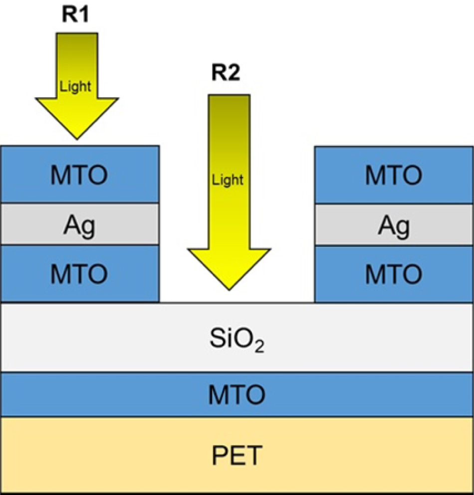
2 different types of films, the MTO/Ag/MTO/PET with SiO2/MTO and the SiO2/MTO/PET (IMLs) only, were prepared on PET to compare the effect of refractive index-mated lays (IMLs), in MTO/Ag/MTO multilayer TCO films. Fig. 1 shows a schematic diagram describing two distinct parts. The typical parts having different mismatched refractive indices, MTO/Ag/MTO/SiO2/MTO/PET and the SiO2/MTO/PET layers, are corres- ponded to the unetched (R1) and the etched (R2), respectively. Thickness of each films were determined by the scanning electron microscope (SEM) and the surface profiler (Alpha-step 500, TENCOR). The surface morphologies and topography were imaged through Atomic force microscopy (Digital Instruments, Nanoscope IIIa). Spectroscopic ellipsometry was used to measure the refractive index and the extinction coefficient of thin films simultaneously in the wavelength range of 400-800 nm. The optical transmittance and reflectance of the multilayer films were determined by UV-VIS spectrophotometer (KONICA MINOLTA CM-3600d) with D65 light source in the wavelength range of 200-700 nm. The electrical resistivity of the films was obtained by using 4-point probe technique. In addition, the elemental distribution along the vertical planes and interfacial diffusion of multilayer film were analyzed by using X-ray photoelectron spectroscopy (Ulvac-PHI, PHI Quantera-II) depth profiler. The film flexibility was evaluated by film bending tester (ZTEC, ZBT-200) under 5 mm curvature radius condition.
|
Fig. 1 A schematic diagram of MTO/Ag/MTO/SiO2/MTO structured film |
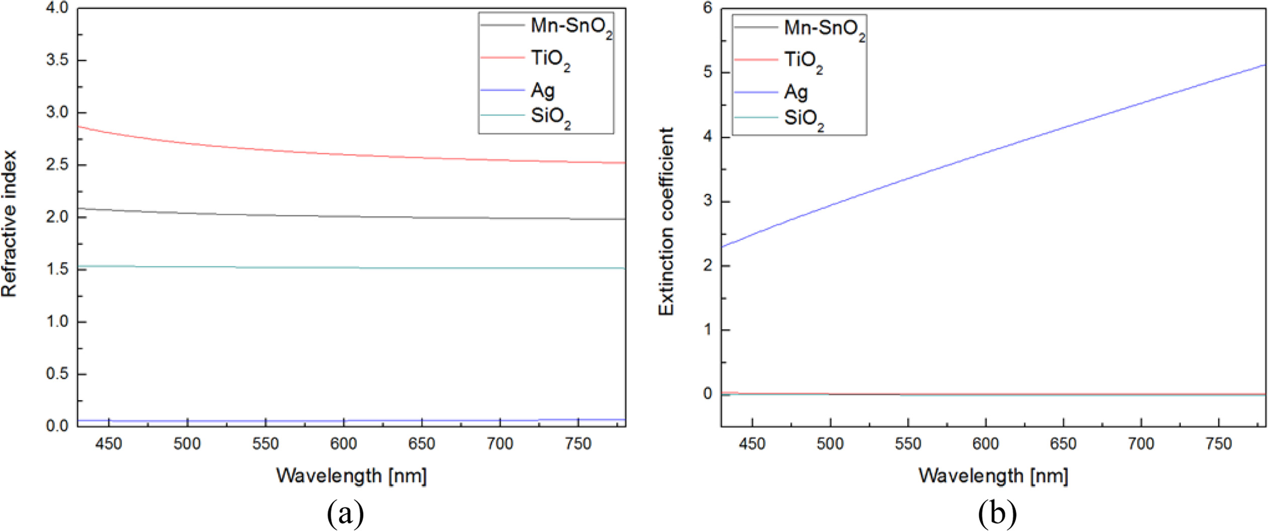
For an accurate analysis from EMP simulation, the refractive index n and extinction coefficient k determined using ellipsometry are necessary. Fig. 2(a) shows the measured dispersion curves for MTO, SiO2 and Ag single layer films deposited on Si wafer in the wavelength range of 400 nm to 800 nm. The obtained refractive indices of MTO, SiO2 and Ag at a wavelength of 550 nm were 2.02, 1.52 and 0.06 respectively, which values are similar to those in previous report [19]. Furthermore, the refractive index of MTO is quite similar to that of SnO2 due to a limited amount of Mn doping (2.59 wt.%). However, the extinction coefficient of MTO, SiO2 and Ag, seen in Fig. 2(b), was nearly 0 except for Ag regardless of wavelength change.
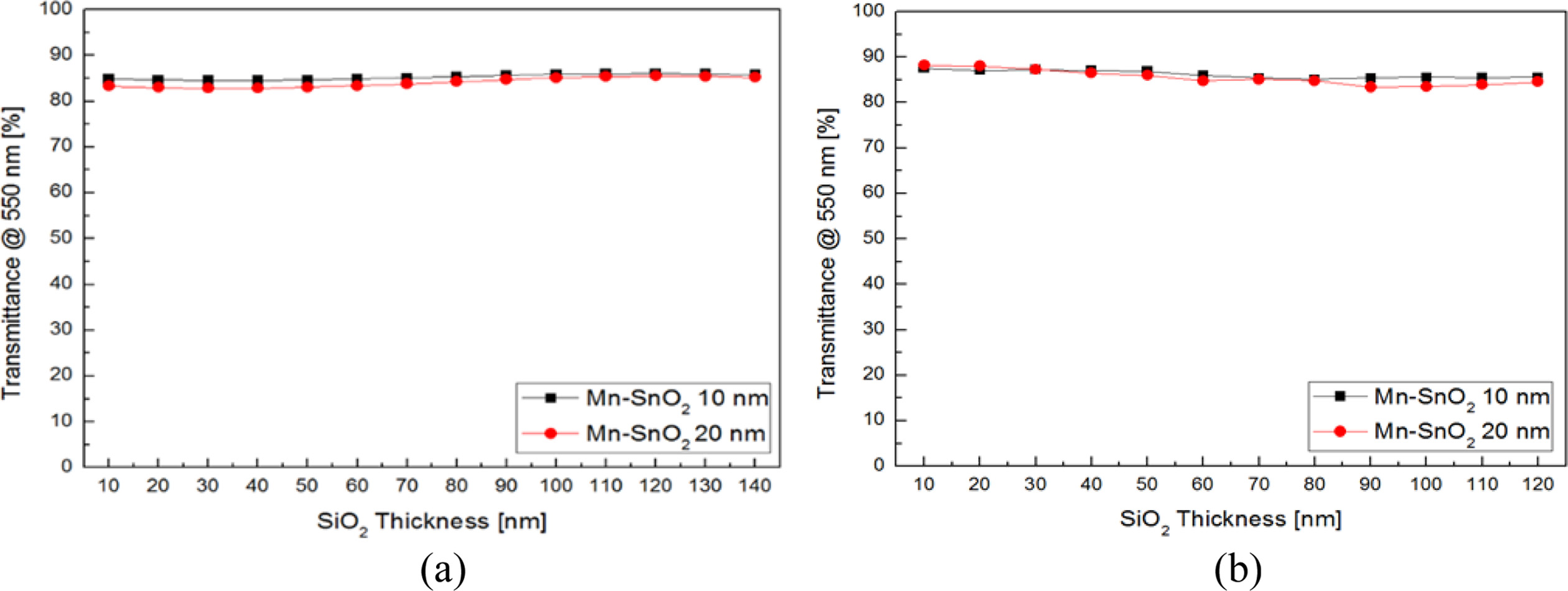
Fig. 3 shows the optical spectra of simulated and experimental transmittance in MTO (40 nm)/Ag (13 nm)/MTO (40 nm)/SiO2 (10-120 nm)/MTO (10-20 nm) film as a function of SiO2 and MTO thicknesses at 550 nm wavelength (Tr550nm). As can be seen from Fig. 3(a), the simulated transmittance has not changed significantly. Only it is seen that the simulated transmittance value was slightly increased with increasing SiO2 thickness. Whereas, the experimental results in Fig. 3(b), Tr550nm of films was gradually decreased from 87.6 to 85.1% in MTO (10 nm) and from 88.2 to 83.4% in MTO (20 nm), with increasing thickness of SiO2 from 10 to 120 nm. The slight deviation of trends between the simulation and the experiment results are presumably associated with the effect of the absorption rise with the increase of SiO2, which is much greater than anti-reflection effect of IMLs [20]. Moreover, deposition temperature was considered to cause crystallinity change and interface instability due to elemental diffusion between the layers of the stackup. In addition, when the MTO thickness in IML was 20 nm, transmittance decline was much higher than MTO (10 nm) specimens at various SiO2 thickness range of 80-120 nm.
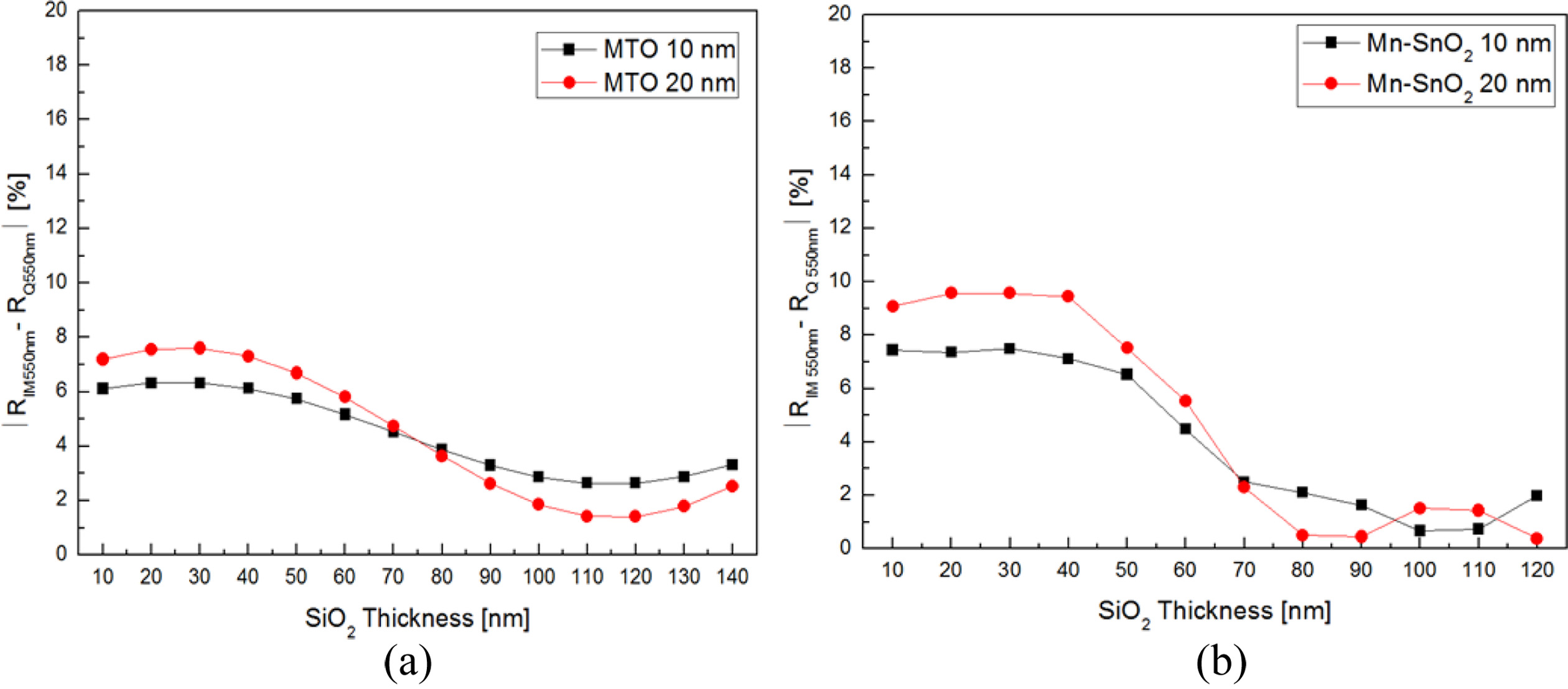
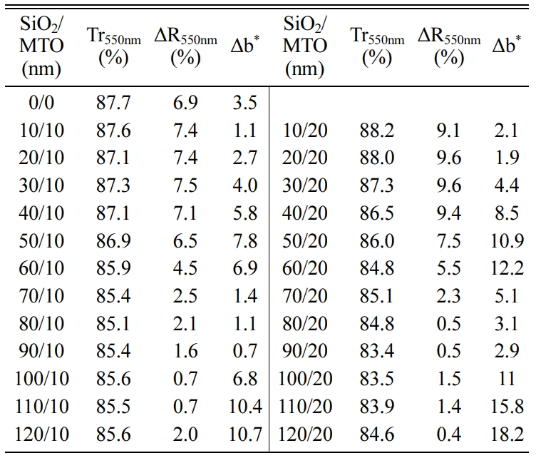
Fig. 4 shows the simulated and experimentally measured reflectance difference (∆R550nm) between the etched (SiO2/MTO/PET) and the unetched (MTO/Ag/MTO/SiO2/MTO/PET) of multilayer films. As seen in Fig. 4, reflectance difference spectra at 550 nm wavelength (∆R550nm) with increasing SiO2 thickness exhibits typical modulated patterns, gradually increased with IMLs (SiO2 and MTO) thickness, reaches a maximum of around 6.3 for simulation and 7.5 for experiment in SiO2 (30 nm)/MTO (20 nm) and then decreased rapidly. However, in contrast to transmittance data, both simulation and experimental spectra of ∆R550nm show quite similar tendency between simulation and experiment spectra and decreased as a function of the SiO2 thickness although the details slight differ. In addition, the designed MTO/Ag/MTO multilayer with SiO2/MTO layers representing excellent ∆R550nm and Tr550nm by experiment are SiO2 (80, 90, 100, 110, 120 and 120 nm)/MTO (10 nm) showing 2.1, 1.6, 0.7, and 2.0%, respectively, which were lower than a MTO/Ag/MTO/PET film without IMLs (∆R550nm = 6.9%). The lowest ∆R550nm of 0.7% was obtained at SiO2 (100 nm)/MTO (10 nm).
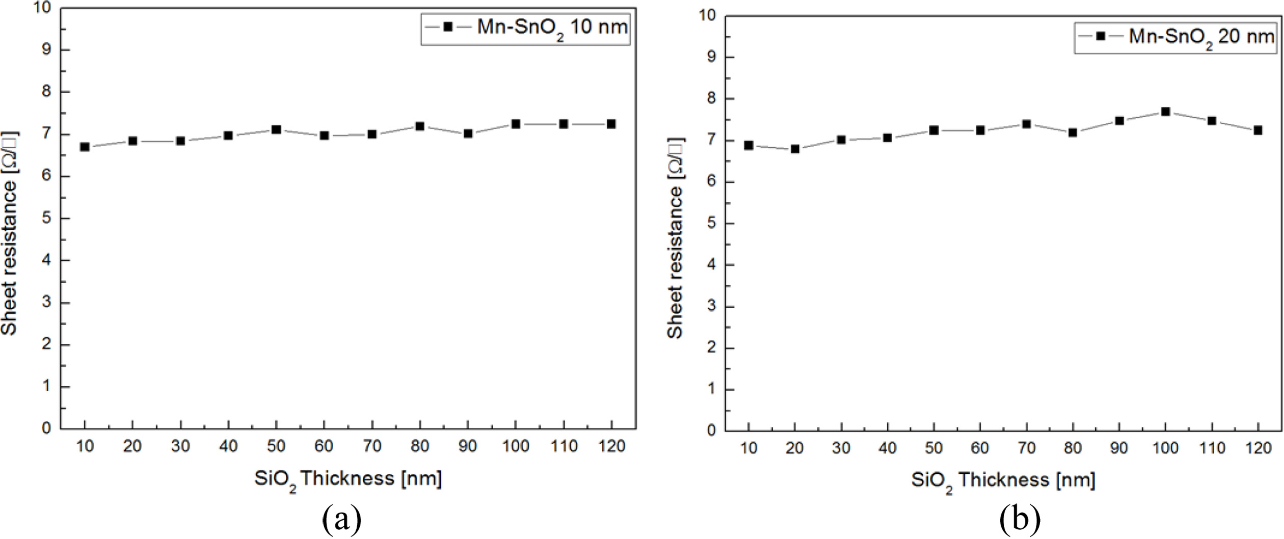
Fig. 5. shows the sheet resistances (Rsh) of MTO (40 nm)/Ag (13 nm)/MTO (40 nm)/SiO2 (10-120 nm)/MTO (10-20 nm) multilayer films depending on SiO2 and MTO thickness. As seen in Fig. 5, sheet resistance remained almost constant, ranging from 6 to 8 Ω/sq., regardless of the SiO2 film thickness change (10-120 nm), although MTO thickness are varied from 10 to 20 nm. Generally, the total sheet resistance of stacked OMO multilayer film is subjected to the dominant effect on the thin embedded Ag layer [21]. Therefore, the resistance was maintained as a result of fixing the thickness of Ag layer (13 nm).
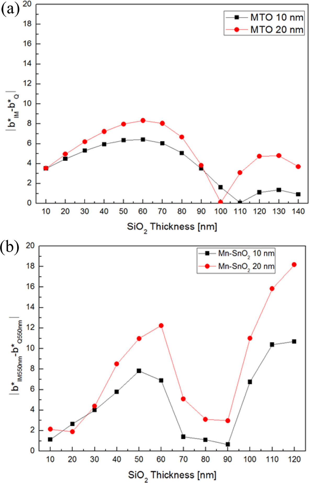
The reflectivity variation can be represented in the CIE L*a*b* color space [22]. The L*a*b* color space describes color appearance by dividing it into three coordinates, L* for lightness and a* and b* for the green-red and blue-yellow, respectively. The yellow/blue colors are represented along the b* axis, with blue at negative b* values and yellow at positive b* values, respectively. Fig. 6 shows the yellow-blue color difference (∆b*) between the etched and the unetched part with different SiO2 thickness. From Fig. 6(a), ∆b* curves shows the similar modulated patterns as compared with the reflectivity spectra. The lowest ∆b* was as low as 0.06 at SiO2 (60 nm)/MTO (10 nm), which is comparable to 3.5 of MTO/Ag/MTO/PET film without IMLs. Table 1 summarized all the optical and pattern visibility properties of MTO (40 nm)/Ag (13 nm)/MTO (40 nm) films depending on the IMLs thickness.
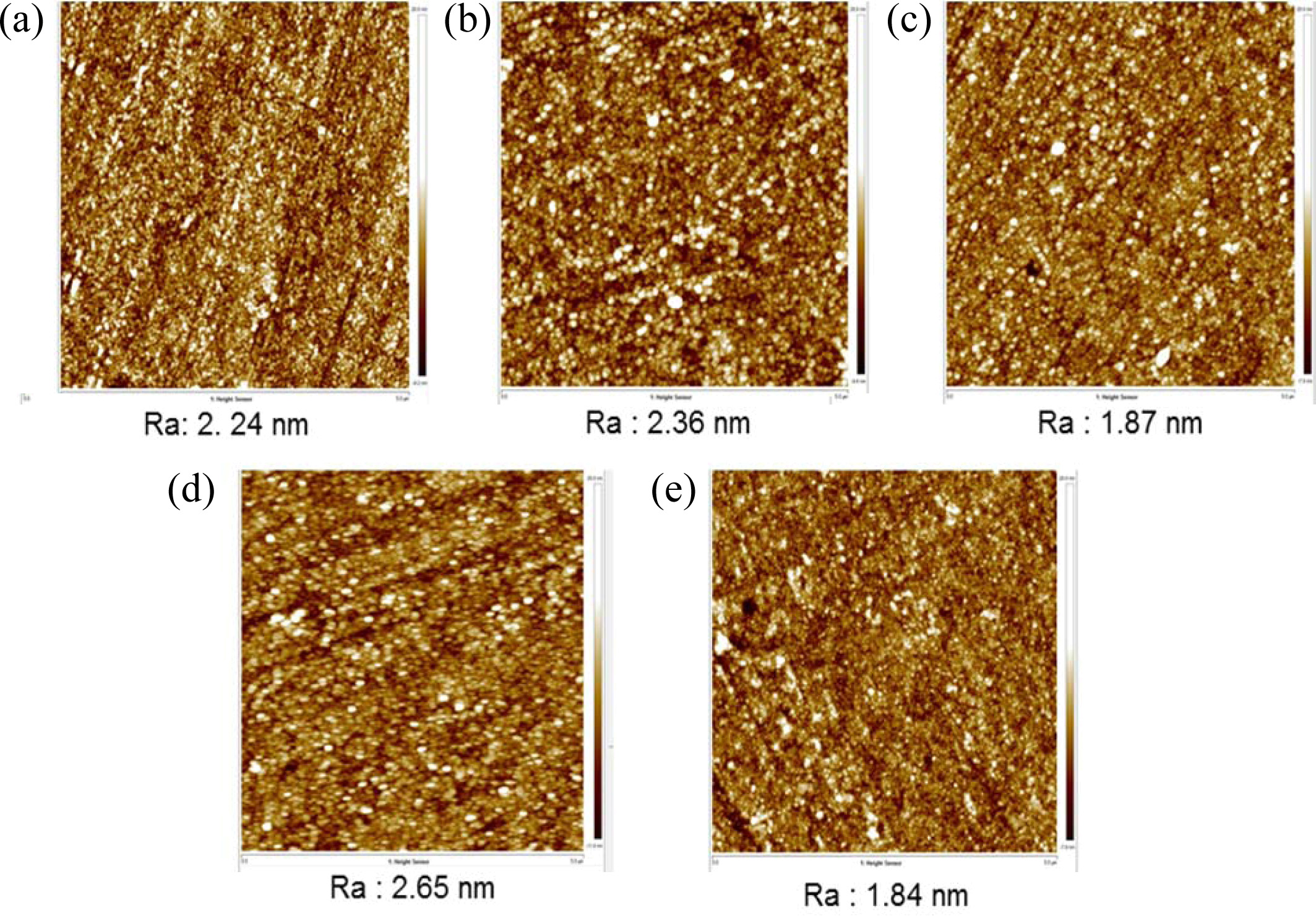
Fig. 7 shows the surface morphologies and roughness of each layer in MTO (40 nm)/Ag (13 nm)/MTO (40 nm) film with SiO2 (90 nm)/MTO (10 nm) film by deposition order. From AFM images, average roughness (Ra) of each layer represents as low as 2.24, 2.36, 1.87, 2.65, and 1,84 nm in order of depositions. It has been suggested that the low Ra can help to improve trans- mittance, because the smooth surface suppresses scatter- ing of the defects.
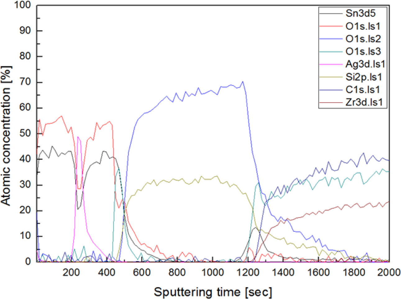
Fig. 8 represents the XPS depth profile result obtained from the optimized MTO (40 nm)/Ag (13 nm)/MTO (40 nm) film with SiO2 (90 nm)/MTO (10 nm) layer. As seen in Fig. 8, the XPS depth profile shows systematical features and well defined top/bottom MTO, Ag, and SiO2 with the same composition and thickness. However, 48% atomic% of Ag3d implies that there was a noticeable interfacial reaction, especially between Ag and MTO layer.
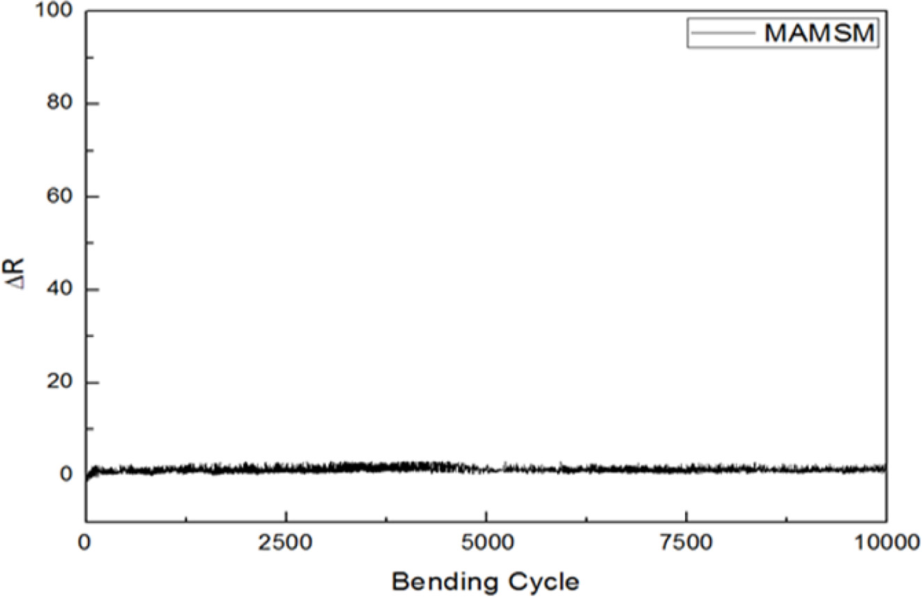
Fig. 9 represents the bending cycle-resistance change (∆R) curve of MTO (40 nm)/Ag (13 nm)/MTO (40 nm) film with SiO2 (90 nm)/MTO (10 nm) layer. The resistance change can be estimated as R-R0, where R0 is the initial resistance and R is the final resistance during the bending test. The value of ∆R for the optimized film remains almost constant after 10,000 cycles. The film resistance was varied from 14.2 to 15.6 Ω, increased approximately 10%. This result implies that the MTO/Ag/MTO/SiO2/MTO multilayer film has the excellent flexibility under the condition of 5 mm inner bending radius.
|
Fig. 2 Measured (a) refractive index and (b) extinction coefficient spectra of MTO, SiO2 and Ag single layer films. |
|
Fig. 3 Transmittance spectra at the 550 nm wavelength of MTO/Ag/MTO/SiO2/MTO multilayer films with different thickness of the SiO2/ MTO; (a) simulation data and (b) experimental data. |
|
Fig. 4 (a) Simulated and (b) experimentally measured reflectance difference (∆R550nm) of MTO/Ag/MTO film with SiO2/MTO layers. |
|
Fig. 5 The sheet resistances (Rsh) of MTO (40 nm)/Ag (13 nm)/MTO (40 nm)/SiO2 (10-120 nm)/MTO (10-20 nm) multilayer films depending on SiO2 and MTO thickness; (a) MTO (10 nm) and (b) MTO (20 nm). |
|
Fig. 6 (a) Simulated and (b) experimental yellow-blue color difference (∆b*) of MTO/Ag/MTO film with SiO2/MTO layers. |
|
Fig. 7 The surface roughness of MTO (40 nm)/Ag (13 nm)/MTO (40 nm) film with SiO2 (90 nm)/MTO (10 nm) layer with deposition order; (a) MTO (10 nm), (b) SiO2 (90 nm)/MTO (10 nm), (c) MTO (40 nm)/SiO2 (90 nm)/MTO (10 nm), (d) Ag (13 nm)/MTO (40 nm)/SiO2 (90 nm)/MTO (10 nm) and (e) MTO (40 nm)/Ag (13 nm)/MTO (40 nm)/SiO2 (90 nm)/MTO (10 nm). |
|
Fig. 8 XPS depth profile of MTO (40 nm)/Ag (13 nm)/MTO (40 nm) film with SiO2 (90 nm)/MTO (10 nm) layer. |
|
Fig. 9 Bending curve of cycle–resistance change of MTO (40 nm)/Ag (13 nm)/MTO (40 nm)/ film with SiO2 (90 nm)/MTO (10 nm) layer under the condition of 5 mm inner bending radius. |
|
Table 1 The optical and pattern visibility properties of MTO (40 nm)/Ag (13 nm)/MTO (40 nm) films depending on the thickness of IM layers |
In this study, we evaluated and compared the effect of two refractive index-matched layers (IMLs), SiO2 and MTO, on the optical spectra and color variation of MTO/Ag/MTO multilayer transparent conducting oxide (TCO) films. In addition, the optical transmittance of the multilayer with IMLs was simulated using the Essential Macleod Program. All the fabricated multilayer films exhibited high optical transmittances above 85% at a wavelength of 550 nm when the thickness of MTO in the IMLs was 10 nm. As compared with a MTO/Ag/MTO/PET film without IMLs (∆R550nm = 6.9%), the designed MTO/Ag/MTO multilayer with SiO2 (80, 90, 100, 110, 120 and 120 nm)/MTO (10 nm) layers represent excellent ∆R550nm and Tr550nm showing 2.1, 1.6, 0.7, and 2.0%, respectively. The lowest ∆b* of 0.06 was obtained at MTO/Ag/MTO film with SiO2 (60 nm)/MTO (10 nm) layers, which is comparable to 3.5 of MTO/Ag/MTO/PET film without IMLs. Therefore, it can be concluded that the IMLs consisting of SiO2/MTO exhibited an anti-reflection effect, which contributed to the improvement in the etched electrode pattern visibility because of the decrease in the reflectance and color variation of the etched part of the multilayer film. Furthermore, the excellent electrical stability and flexibility of multilayer film was obtained because the resistance change rate of selected multilayer film exhibits about 10%. after 10,000 bending cycles with inner curvature radius of 5 mm. The results of our study indicate that about 2% range of reflectivity and color variation of the MTO/Ag/MTO/SiO2/MTO multilayer film could be possibly applied to reduce the pattern visibility in optoelectronic devices.
This research was supported by Chungbuk National University Korea National University Development Project (2020).
- 1. K. Ellmer, Nat. Photonics 6[12] (2012) 809-817.
-

- 2. A. Stadler, Materials 5[12] (2012) 661-683.
-

- 3. H. Liu, V. Avrutin, N. Lzyumskaya, U. Ozgar, H. Morkoc, Superlattices Microst. 48[5] (2010) 458-484.
-

- 4. F. Liang, Z. Ying, Y. Lin, B. Tu, Z. Zhang, Y. Zhu, H. Pan, H. Li, L. Luo, O. Ageev, and Z. He, Adv. Mater. Interfaces 7[20] (2020) 2000591.
-

- 5. D.H. Choi, H.J. Seok, D.H. Kim, S.K. Kim, and H.K. Kim, Sci. Technol. Adv. Mater. 21[1] (2020) 435-449.
-

- 6. O. Akdemir, M.Z. Borra, H. Nasser, R. Turan, and A. Bek, Int. J. Energy Res. 44[4] (2020) 3098-3109.
-

- 7. Y. Sugimoto, K. Igarashi, S. Shirasaki, and A. Kikuchi, Phys. Status Solidi. C 13[7-9] (2016) 568-571.
-

- 8. H. Kong and H.Y. Lee, Thin Solid films 696 (2019) 137759.
-

- 9. H.J. Jo, J.-H. Yang, S.-W. Choi, J.H. Park, E.J. Song M.H. Shin, J.H. Ahn, and J.-D. Kwon, Sol. Energy Mater. Sol. Cells 202 (2019) 110131.
-

- 10. C.Y. Tsay and S.C. Liang, J. Alloys Compd. 622 (2015) 644-650.
-

- 11. J.J. Lee, J.Y. Ha, W.K. Choi, Y.S. Cho, and J.W. Choi, ACS Comb. Sci. 17[4] (2015) 247-252.
-

- 12. S.M. Yoon, T.K. Kim, and G.E. Jang, Phys. Status Solidi A 215[20] (2018) 1700974.
-

- 13. S.M. Yoon, J.I. Choi, and G.E. Jang, J. Nanosci. Nanotechnol. 17[10] (2017) 7218-7222.
-

- 14. G. Haacke, J. Appl. Phys. 47[9] (1976) 4086-4092.
-

- 15. C.H. Hong, J.H. Shin, B.K. Ju, K.H. Kim, N.M. Park, B.S. Kim, and W.S. Cheong, J. Nanosci. Nanotechnol. 13[11] (2013) 7756-7759.
-

- 16. R. Leitel, O. Stenzel, S. Wilbrandt, D. Gäbler, V. Janicki, and N. Kaiser, Thin Solid Films 497[1-2] (2016) 135-141.
-

- 17. X. Yan, F.W. Mont, D.J. Poxson, M.F. Schubert, J.K. Kim, J. Cho, and E.F. Schubert, Jpn. J. Appl. Phys. 48[12] (2009) 120203.
-

- 18. J.G. Kim, S.M. Yoon, and G.E. Jang, J. Ceram. Process. Res. 17[2] (2016) 80-84.
- 19. R.D. Shannon, R.C. Shannon, O. Medebach, and R.X. Fischer, J. Phys. Chem. Ref. Data 31[4] (2002) 931-970.
-

- 20. J.D. Winans, C. Hungerford, K. Shome, L.J. Rothberg, and P. M. Fauchet, Opt. Express 23[3] (2015) A92.
-

- 21. S. Singh, V. Sharma, S. Surbhi, D. Saini, K. Asokan and K. Sachdev, Ceramic Inter. 43[13] (2017) 9759-9768.
-

- 22. ASTM, in Proceedings of Symposium on Color--its Speci- fication and Use in Evaluating the Appearance of Materials, (American Society for Testing Materials, 1941) p.3.
 This Article
-
2021; 22(1): 114-120
Published on Feb 28, 2021
- 10.36410/jcpr.2021.22.1.114
- Received on Nov 27, 2020
- Revised on Dec 15, 2020
- Accepted on Dec 29, 2020
 Services
- Abstract
introduction
experimental
results and discussion
conclusions
- Acknowledgements
- References
- Full Text PDF
Shared
 Correspondence to
- Guneik Jang
-
Department of Materials Engineering, Chungbuk National University
Tel : +82-43-261-2412 Fax: +82-43-271-3222 - E-mail: gejang@chungbuk.ac.kr


 Copyright 2019 International Orgranization for Ceramic Processing. All rights reserved.