- Structural and electrical properties of Ba(Sr,Ti)O3/K(Ta,Nb)O3 multilayer thin film for the application of electro-caloric devices
Min-Su Kwona, Sung-Gap Leea,*, Kyeong-Min Kima and Seungkeun Choib
aDept. of Materials Engineering and Convergence Technology, ERI, Gyeongsang National University, Jinju 52828, Korea
bSchool of STEM, Univ. of Washington, Bothell, WA, 98011, USA
In this study, the
multilayered thin films of (Ba,Sr)TiO3/K(Ta,Nb)O3 were
fabricated by the sol-gel and spin coating methods, and their structural and
electrical properties were investigated. The specimen showed polycrystalline
X-ray diffraction (XRD) characteristics with a tetragonal structure. The
average grain size and film thickness for one coating were about 30~40nm and
60nm, respectively. The phase transition temperature of specimen was lower than
10 oC. The dielectric constant and loss at 20 oC
of the specimen coated six times were 1,231 and 0.69, respectively. The rate of
change in dielectric constant at an applied direct current (DC) voltage of the
six times coated thin films was 17.3%/V. The electrocaloric effect was the
highest around the temperature at which the remanent polarization rapidly
changed. When an electric field of 660kV/cm was applied to the triply coated
thin films, the highest electrocaloric property of 4.41 oC was
observed.
Keywords: Ba(Sr,Ti)O3, K(Ta,Nb)O3, Multilayer thin film, Ferroelectric effect, Electro-caloric effect, Remanent polarization, Interface properties.
BaTiO3 ceramics with ABO3 perovskite
crystal structure is a typical ferroelectric material and has been
studied for application to various devices such as capacitors, piezoelectric
transducers, and infrared sensors using excellent structural and electrical
properties [1,2]. Also, K(Ta,Nb)O3 ceramics with the same
perovskite structure have been studied for application to electro-optic
devices, memory devices, and sensors by using various
structural characteristics and electrical properties depending
on the composition ratio of Ta and Nb [3,4]. Recently, BaTiO3
and K(Ta,Nb)O3 ceramics have attracted
attention as lead-free materials as environmental issues
become important social issues.
Studies on thin films have mainly been focused on the
changes in the manufacturing process and improvement of properties
of materials [5,6]. Also, research on the interfacial phenomenon of thin
film devices has mainly focused on the interface between substrate and thin film
[7]. Multilayer thin films, which have been stacked alternately
with different composition or materials, exhibit excellent
electrical properties due to the formation of super-lattice structures or
mixture compositions in the interfacial layer through epitaxial growth.
However, studies on the various electronic properties occurring at the
interface by laminating different materials have been carried out only in part,
despite a theoretical possibility.
Electronic devices have become more sophisticated and
complex, and devices are becoming more and more micronized. As a result, heat
generation problems in circuits and devices are recognized as important factors affecting the
performance of devices. The problems of heat
generation of devices are generally solved by using a heat dissipation
properties of substrates, but it is limited in performance and price. Recently,
as the need for cooling solutions for micro- or nanoelectronic devices with
high power or high density heat generation has increased, research has been
actively conducted on the electrocaloric effect in ferroelectric materials
using small and highly energy efficient properties. In 2005, A. S. Mischenko et
al. [9] reported a study on the application on ferroelectric Pb(Zr0.95Ti0.05)O3
thin films as cooling devices using electrocaloric
characteristics. However, since Pb(Zr,Ti)O3-based materials have a phase transition
temperature higher than 240 oC, applications of cooling devices
at room temperature are limited, and researches have been limited by
environmental problems caused by Pb element.
In this study, (Ba,Sr)TiO3/K(Ta,Nb)3
(BST/KTN) multilayer thin films were prepared by alternately laminating of
lead-free (Ba,Sr)TiO3 and K(Ta,Nb)O3 thin films And their
structural and electrical properties were investigated according to the number
of coatings of the specimens in order to investigate the application as cooling
devices.
(Ba0.7Sr0.3)TiO3 (BST)
and K(Ta0.6Nb0.4)O3 (KTN) with low phase
transition temperature were selected to investigate
the feasibility of the application as an cooling elements
capable of operating at room temperature [10,11].
BST precursor solutions were prepared by the sol-gel
method from barium acetate (Junsei Chemical Co., Japan, 99.0%), strontium
acetate 0.5-water (KANTO Chemical Co., Japan, 99.0%), titanium
(IV) iso-propoxide (Junsei Chemical Co., Japan, 99.0%),
as starting materials, with acetic acid and
2-methoxyethanol as solvents. And KTN precursor solutions were synthesized from
potassium acetate (CH3COOK, Sigma Aldrich, 99%), niobium
ethoxide (Nb(COH2CH3)5, Alfa aesar, 99.999%),
tantalum ethoxide (Ta(COH2CH3)5, Alfa aesar,
99.999%) with 2-methoxyethanol used a solvent. The molar con- centration of solution was adjusted to 0.3
M, and 10 mol% of excess potassium acetate was added to compensate for the expected K2O
losses during annealing.
BST/KTN multilayer thin films
were prepared by alternately coated BST and
KTN. Especially, to suppress ion diffusion at interface between thin films and
Pt/Ti/SiO2/Si substrates, BST thin films having excellent chemical
stability were coated on the substrate as the first layer. Structural and
electrical properties of BST/KTN multilayer thin films were investigated
according to the number of coatings.
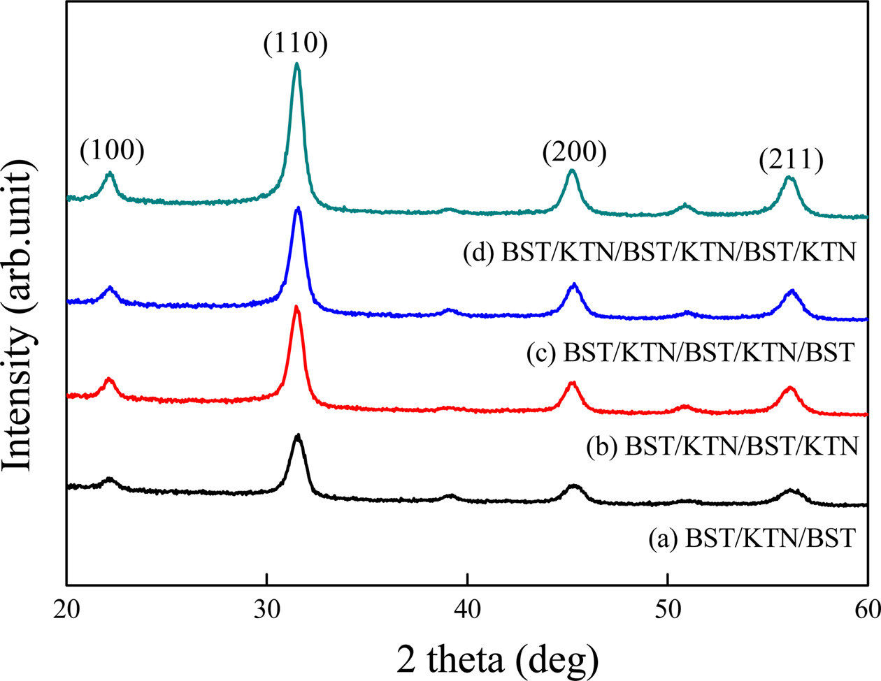
Fig. 1 shows X-ray diffraction (XRD) patterns of BST/KTN
multilayer thin films according to the number of coatings.
BST and KTN thin films were repeatedly coated from 3
times to 6 times on Pt/Ti/SiO2/Si substrates. Generally, single KTN
thin films were observed with a secondary phase such as K2Ta2O6
pyrochlore phase. However, in this study,
all specimens showed homogeneous
polycrystalline XRD patterns with tetragonal structure. This is because the BST
thin film coated with the first layer acts as a seed layer for KTN upper layer
crystal- lization and the crystal
structure of ABO3 perovskite having the same BST thin film and KTN
thin film [12]. As the number of coatings increased, crystallinity of
multilayer thin films improved as increasing XRD peaks intensities and
decreasing FWHM (full width at half maximum) values.
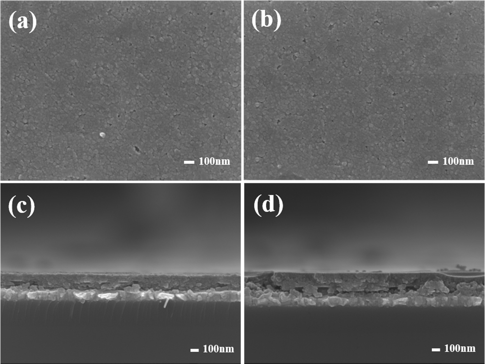
Fig. 2 shows surface and cross-sectional microstructures
of BST/KTN multilayer thin films according to the number of
coatings. All specimens showed dense crystal structure
composed of small and homogeneous grains, and average
grain size was about 30~40 nm. In general, KTN thin
films are difficult to fabricate specimens with homogeneous structure due to
high vapor pressure characteristics of K ions, and many pores are
distributed [13]. However, BST/KTN multilayer thin films showed
homogeneous and dense microstructure, probably due to the microstructure of the
lower BST thin film acting as the nucleation site of the upper KTN thin film.
Average thickness for one-time coated thin films was about 60 nm.
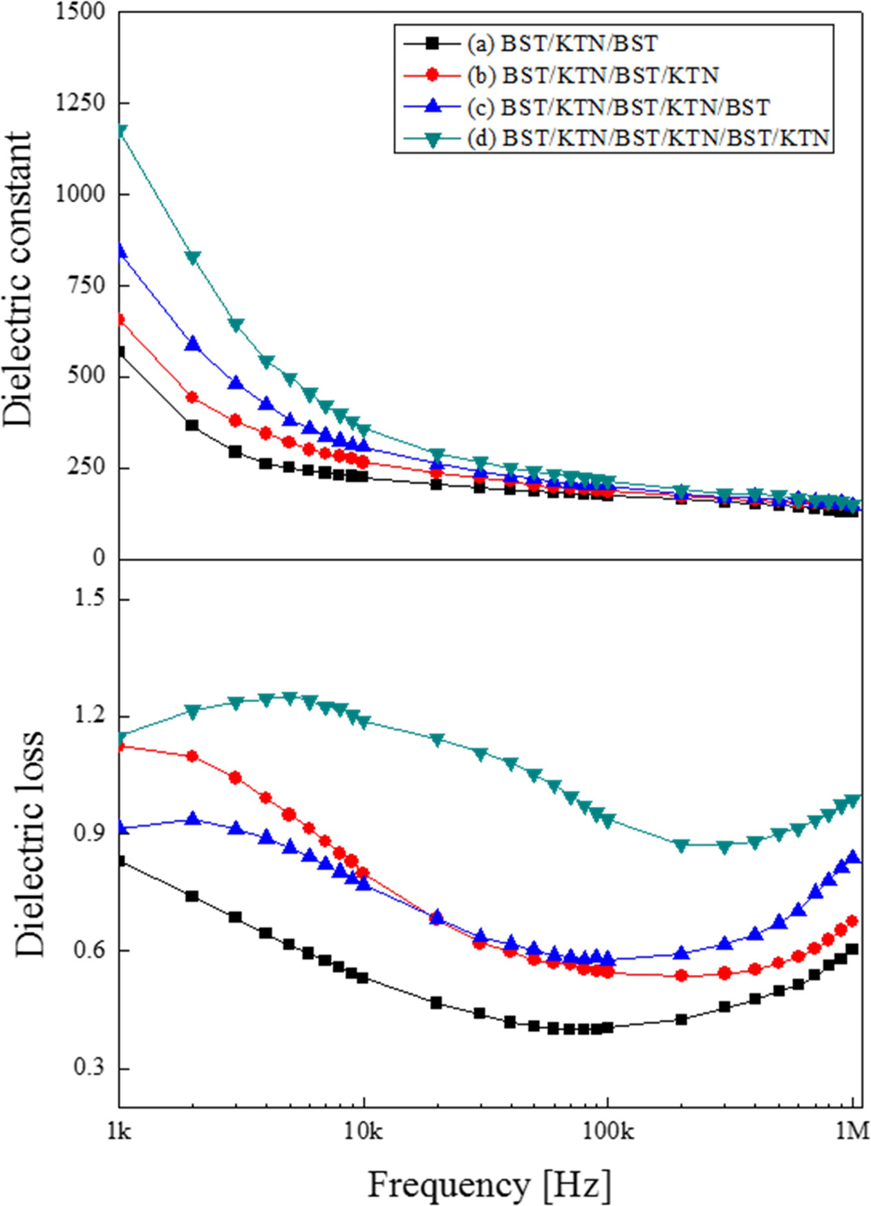
Fig. 3 shows dielectric constant and dielectric loss of BST/KTN
multilayer thin films with frequency application. All
specimens showed the typical dielectric relaxation characteristics [14].
Dielectric constant and dielectric loss increased with increasing the number of
coatings. This is probably due to the decrease in the stress on interfaces due
to the difference in lattice constant between Pt substrate and BST thin film.
Also, as the number of coatings increased, the slope of decrease in dielectric
constant with increasing frequency was increased due to the distribution of
space charge formed at interfaces between BST and KTN thin films [15, 16].
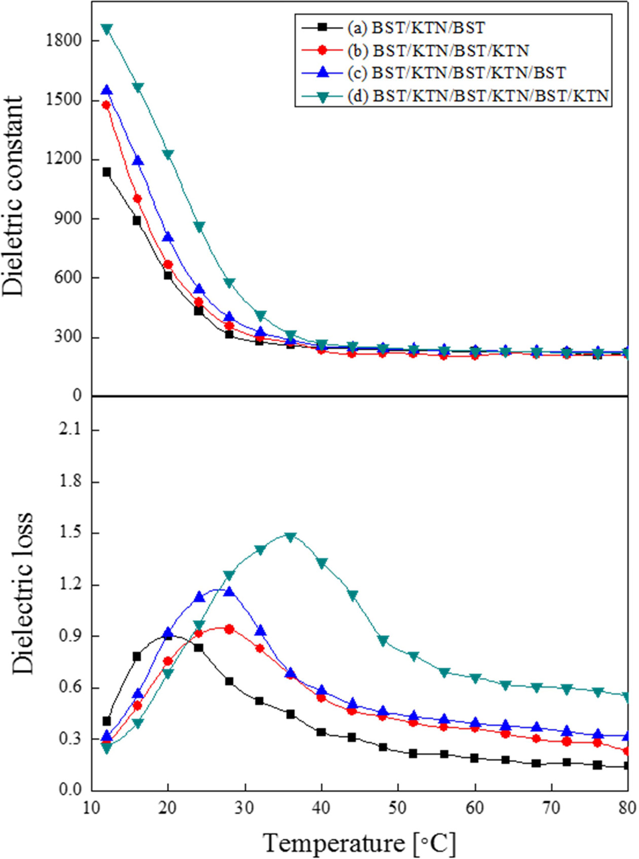
Fig. 4 shows dielectric constant and dielectric loss of BST/KTN
multilayer thin films with temperature variation.
Dielectric constant and dielectric loss increased as the
number of coatings increased. This is attributed to the formation of
interfacial polarization due to space charge between BST and KTN thin films
[17]. Also, it is considered that dielectric constant decreased with increasing
temperature in the measurement temperature range of 10~80 oC
because the phase transition tem-
peratures were located below 10 oC. Dielectric constant
and dielectric loss of the 6 coated BST/KTN multilayer thin films at 20 oC
were 1,231 and 0.69, respectively.
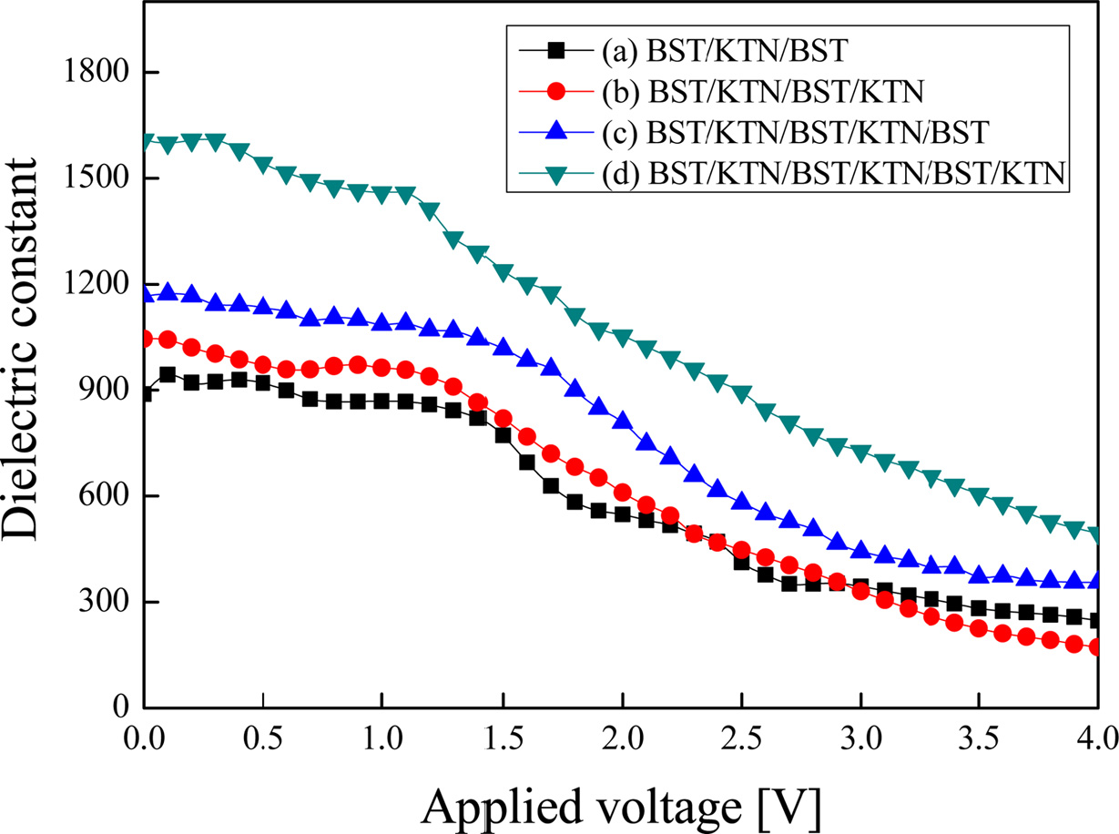
Fig. 5 shows dielectric constant of BST/KTN multilayer
thin films with DC voltage applied. Dielectric constant decreased with
increasing DC applied voltage, which is considered to be due to the suppression
of the displacement of ions [18]. As the
number of coating increased, the distribution of space charge formed between BST
thin film and KTN thin film and the dependence on DC electric field increased,
so the rate of decrease of dielectric constant according to the applied voltage
increased. The 6 coated BST/KTN multilayer thin films showed the highest change
rate of 17.3%/V.
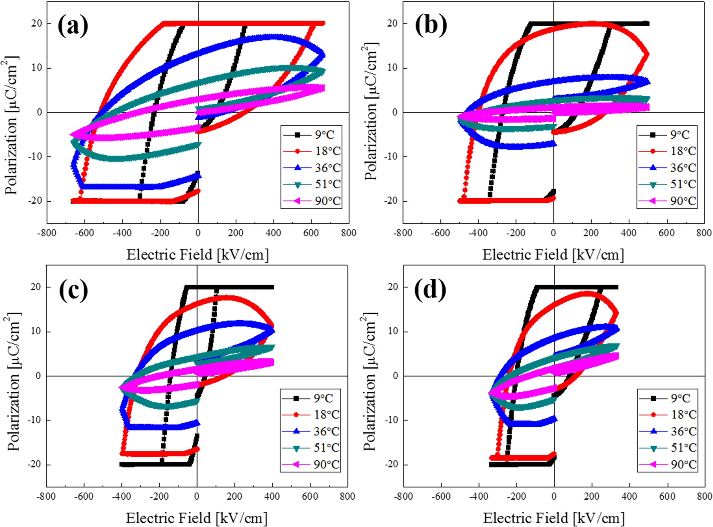
Fig. 6 shows hysteresis loops of BST/KTN multilayer
thin films with the number of coatings and temperature. As the temperature and
the number of coatings increased, remanent polarization and the coercive field
decreased. As shown in Fig. 4, because the phase transition temperature of
specimens were distributed below 10 oC, the
phase structure of BST/KTN multilayer thin films gradually changed
to the paraelectric phase as the temperature increased. Also, it is considered
that the influence of the stress formed at the interface between thin films and
Pt substrate decreased with increasing the thickness of thin films.
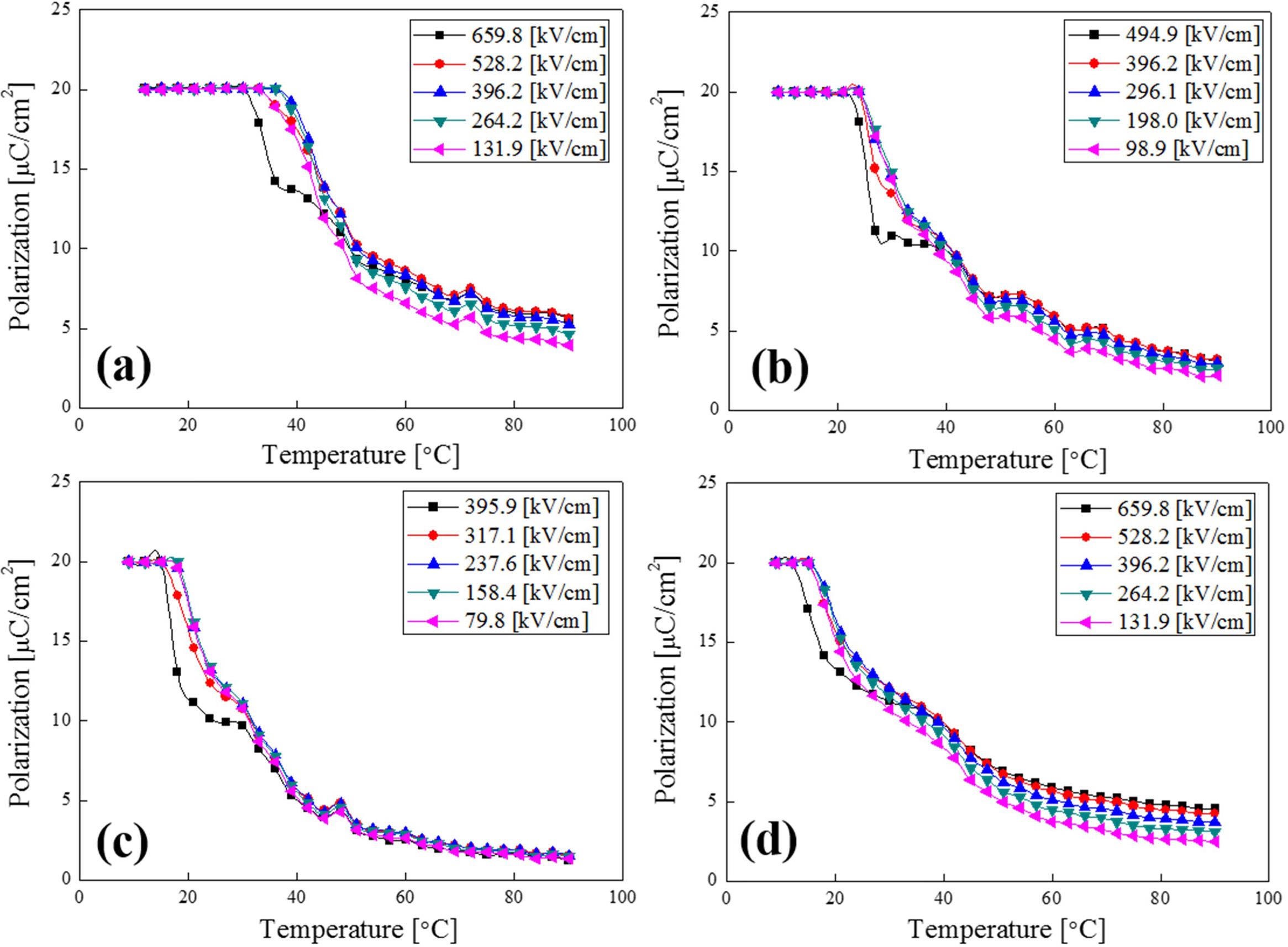
Fig. 7 shows remanent polarization of BST/KTN multilayer
thin films with temperature change. Remanent polarization
measured at 10 °C were fixed at a maximum value and
then the temperature dependent properties were shown. As the number of coatings
increased, temperatures at which remanent polarization rapidly decreased were
shifted to the lower temperature side, and the rate of change of remanent
polarization was decreased with temperature. This is because the
volume ratio of BST and KTN having a phase transition
temperature lower than room temperature increased as the number of coatings
increased, as shown in Fig. 4 and 6.
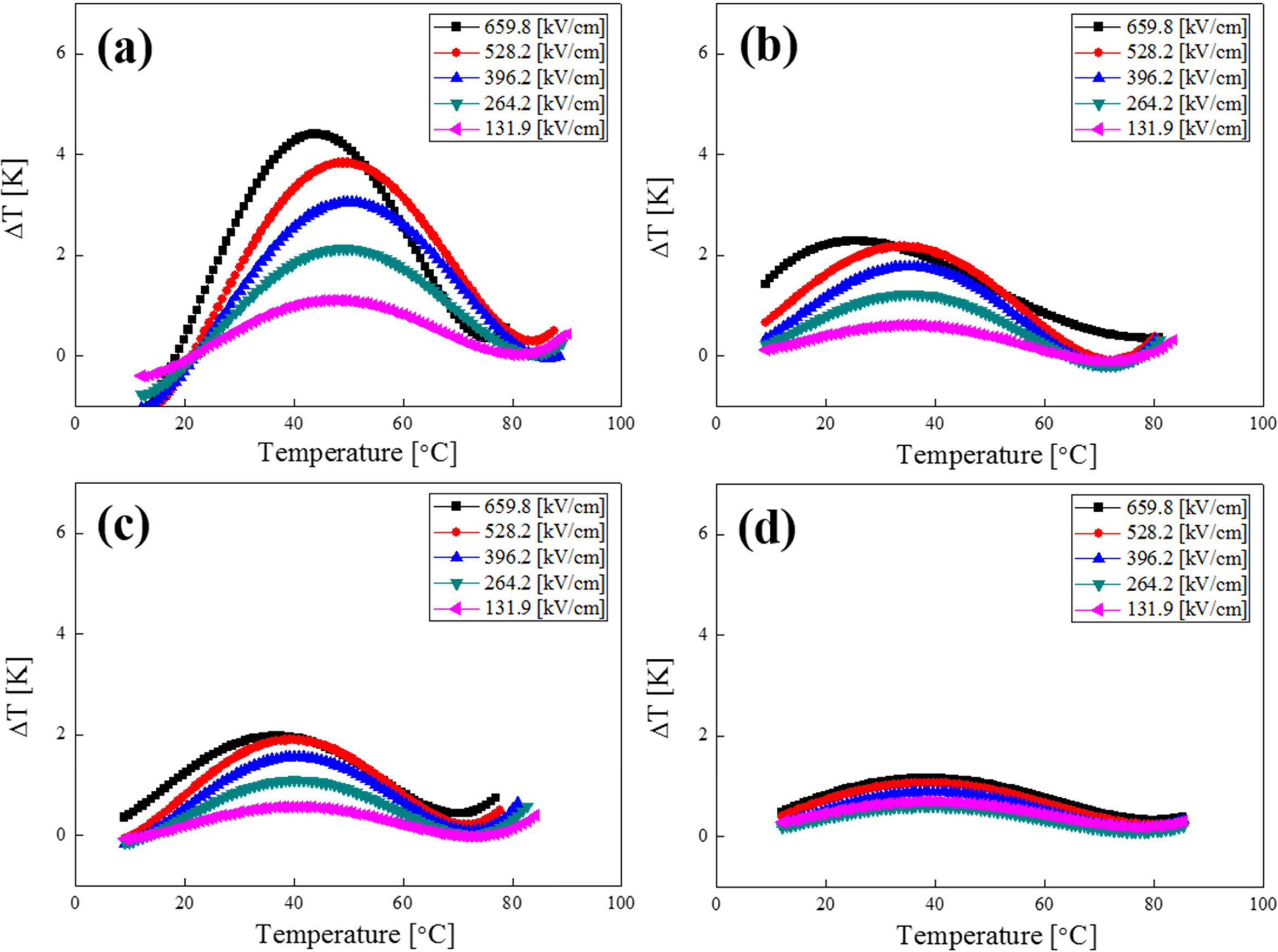
Fig. 8 shows electrocaloric
properties (ΔT) of BST/KTN multilayer thin films according to temperature and
applied voltage. Electrocaloric properties showed the highest values at the temperature where the
remanent polarization rapidly changes.
Electrocaloric properties increased with increasing the applied electric field.
This is probably due to the decrease in entropy and the temperature dependence
of dipoles arrangement as the displacement of dipoles increased when an
electric field was applied near the phase transition [19]. When the electric
field of 660 kV/cm was applied to the 3 times coated BST/KTN multilayer thin films, the
highest electrocaloric property of
4.41 oC was shown.
|
Fig. 1 X-ray diffraction patterns of BST/KTN multilayer thin films with the variation of the number of coatings. |
|
Fig. 2 Surface and cross-sectional microstructures of BST/KTN multilayer thin films with the variation of the number of coatings; (a) surface-3 times, (b) surface-4 times, (c) cross-sectional-3 times, and (d) cross-sectional-4 times. |
|
Fig. 3 Dielectric constant and dielectric loss of BST/KTN multilayer thin films with the variation of frequency. |
|
Fig. 4 Dielectric constant and dielectric loss of BST/KTN multilayer thin films with the variation of temperature. |
|
Fig. 5 Dielectric constant of BST/KTN multilayer thin films with the variation of DC voltage applied. |
|
Fig. 6 Hysteresis loops of BST/KTN multilayer thin films with the variation of the number of coatings and temperature. |
|
Fig. 7 Remanent polarization of BST/KTN multilayer thin films with the variation of temperature. |
|
Fig. 8 Electrocaloric properties (ΔT) of BST/KTN multilayer thin films with the variation of temperature and applied voltage. |
BST/KTN multilayer thin films were prepared by alternately
coating (Ba,Sr)TiO3 thin films and K(Ta,Nb)O3 thin
films. Structural and electrical properties were measured according to the
number of coatings. All specimens showed homogeneous dense polycrystalline microstructure
without secondary phase such as K2Ta2O6
pyrochlore phase. This indicates that BST thin film coated on the Pt/Ti/SiO2/Si
substrate as the seed layer for the upper layer crystallization. Dielectric
constant and dielectric loss increased with increasing the number
of coatings. It is considered that the influence on the stress formed at the
interface due to the difference in lattice constant between Pt substrate and
BST thin film was reduced. As an applied DC voltage increased, dielectric
constant decreased as the displacement of the space charge was suppressed.
Electrocaloric properties showed the highest value near the temperature at
which the remanent polarization suddenly changed, and it increased as the
applied electric field increased.
This research was supported by Basic Science Research
Program through the National Research
Foundation of Korea
(NRF) funded by the Ministry of Education (No. 2017R1D1A3 B03032164) and by the
Gyeongsang National University Fund for Professors on Sabbatical Leave, 2018
and by Korea Institute of Planning and Evaluation
for Technology in Food, Agriculture, Forestry and
Fisheries (IPET) through Agriculture, Food and Rural Affairs
Research Center Support Program, funded by Ministry
of Agriculture, Food and Rural Affairs (MAFRA)(717001-7).
- 1. H. Kishi, Y. Mizuno, and H. Chazono, Jpn. J. Appl. Phys. 42 (2003) 1-15.
-

- 2. A.S. Bhalla, R. Guo, and R. Roy, Mater. Res. Innov. 4[1] (2000) 3-26.
-

- 3. B. Liu, X. Wang, Y. Zhang, X. Lv, and Y. Yang, Ionics 20[12] (2014) 1795-1799.
-

- 4. S. Glinšek, I. Arčon, B. Malič, A. Kodre, and M. Kosec, J. Solgel. Sci. Technol. 62[1] (2012) 1-6.
-

- 5. S. Sharma, A. Kumar, V. Gupta, and M. Tomar, Vacuum 160 (2019) 233-237
-

- 6. C.M. Raghavan, J.Y. Choi, and S.S. Kim, Ceram. Int. 42[8] (2016) 9577-9582.
-

- 7. W. Hu, C. Yang, W. Zhang, G. Liu, and D. Dong, J. Solgel. Sci. Technol. 39[3] (2006) 293-298.
-

- 8. H. Sui, H. Sun, X. Liu, D. Zhou, and R. Xu, J. Eur. Ceram. Soc. 38[16] (2018) 5382-5387.
-

- 9. A.S. Mischenko, Q. Zhang, J.F. Scott, R.W. Whatmore, and N.D. Mathur, Science 311 (2006) 1270-1271.
-

- 10. M.W. Cole, C. Hubbard, E. Ngo, M. Ervin, M. Wood, and R.G. Geyer, J. Appl. Phys. 92[1] (2002) 475-483.
-

- 11. A. Nazeri, M. Kahn, B. Bender, and C. Allen, J. Am. Ceram. Soc. 194445 (1993) 2450-2454.
-

- 12. T. Ohno, M., Fujimoto, T. Ota, M. Fuji, M. Takahashi, and H. Suzuki, J. Eur. Ceram. Soc. 26[10-11] (2006) 2143-2146.
-

- 13. B. Tunaboylu, S.R. Sashital, P. Harvey, S.C. Esener, and A. Bhalla, Ferroelectrics Lett. 28[3-4] (2001) 75-84.
-

- 14. Ch. Rayssi, S. El. Kossi, J. Dhahri, and K. Khirouni, RSC Adv. 8 (2018) 17139.
-

- 15. S. Dash, R.N.P. Choudhary, P.R. Das, and A. Kumar, Canadian Journal of Physics 93 (2015) 738.
-

- 16. G. Abadias, E. Chason, J. Keckes, M. Sebastiani, G.B. Thompson, E. Barthel, G.L. Doll, C.E. Murray, C.H. Stoessel, and L. Martinu, J. Vac. Sci. Technol. A 36 (2018) 020801.
-

- 17. C.C. Wang, M. He, F. Yang, J. Wen, G.Z. Liu, and H.B. Lu, Appl. Phys. Lett. 90[19] (2007) 0-3.
-

- 18. A.E.R. Mahmoud, A.S. Afify, and S.K.S. Parashar, J. Mater. Sci.: Mater. Electron. 30[3] (2019) 2659-2668.
-

- 19. Z. Luo, D. Zhang, Y. Liu, D. Zhou, Y. Yao, C. Liu, B. Dkhil, X. Ren, and X. Lou, Appl. Phys. Lett. 105[10] (2014) 102904.
-

 This Article
-
2019; 20(6): 603-608
Published on Dec 31, 2019
- 10.36410/jcpr.2019.20.6.603
- Received on Jul 1, 2019
- Revised on Oct 4, 2019
- Accepted on Oct 20, 2019
 Services
- Abstract
introduction
experimental
results and discussion
conclusions
- Acknowledgements
- References
- Full Text PDF
Shared
 Correspondence to
- Sung-Gap Lee
-
Dept. of Materials Engineering and Convergence Technology, ERI, Gyeongsang National University, Jinju 52828, Korea
Tel : +82-55-772-1687 - E-mail: lsgap@gnu.ac.kr


 Copyright 2019 International Orgranization for Ceramic Processing. All rights reserved.