


- MIT characteristic of VO2 thin film deposited by ALD using vanadium oxytriisopropoxide precursor and H2O reactant
Changhee Shina, Namgue Leea, Hyeongsu Choib, Hyunwoo Parkb, Chanwon Jungb, Seokhwi Songb, Hyunwoo Yukb, Youngjoon Kimb, Jong-Woo Kimb, Keunsik Kimb, Youngtae Choib, Hyungtak Seoc,*, and Hyeongtag Jeona,b,*
aDivision of Nanoscale Semiconductor Engineering, Hanyang University, Seoul, Korea
bDivision of Materials Science and Engineering, Hanyang University, Seoul, Korea
cDepartment of Materials Science and Engineering and Department of Energy Systems Research, Ajou University, Suwon, Korea
VO2 is an attractive candidate as a transition metal oxide switching material as a selection device for reduction of sneak-path current. We demonstrate deposition of nanoscale VO2 thin films via thermal atomic layer deposition (ALD) with H2O reactant. Using this method, we demonstrate VO2 thin films with high-quality characteristics, including crystallinity, reproducibility using X-ray diffraction, and X-ray photoelectron spectroscopy measurement. We also present a method that can increase uniformity and thin film quality by splitting the pulse cycle into two using scanning electron microscope measurement. We demonstrate an ON / OFF ratio of about 40, which is caused by metal insulator transition (MIT) of VO2 thin film. ALD-deposited VO2 films with high film uniformity can be applied to next-generation nonvolatile memory devices with high density due to their metal-insulator transition characteristic with high current density, fast switching speed, and high ON / OFF ratio.
Keywords: Atomic layer deposition, Vanadium dioxide, Metal insulator transition, Sneak-path current, Selection device
Non-volatile memory (NVM) is widely used in many industrial fields for flash memory applications. However, NVMs are expected to encounter technical limitations in the near future due to the demands of miniaturization, speed, and density. Thus, many researchers have pursued development of next-generation NVMs, such as resistive random-access memory (ReRAM), phase change random-access memory (PCRAM), and magnetic random-access memory (MRAM). ReRAM in particular has good prospects as next-generation non-volatile memory due to its fast switching speed, endurance, and low power consumption. Moreover, as ideal 4F2 (F is the critical feature size, i.e., pattern size, of the gate in the device) memory cell size is possible when using a ReRAM device of cross-point array-type. However, cross-point array-type ReRAM devices contain undesired sneak-path leakage currents that enter the circuit and cause interference. To solve this problem of unipolar ReRAM devices by connecting memory cells, oxide-based selection devices like Schottky diodes, p-n junction diodes, and threshold-type switching devices are used [1-8]. However, solutions to leakage current problems have yet to be developed for bipolar ReRAM devices.
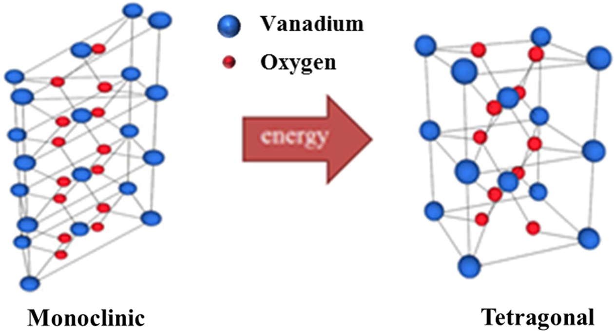
It is necessary to find appropriate selection devices, such as Zener diodes, complementary resistive switches, nonlinear conduction selection devices, and metal-insulator transition (MIT) materials, for cross-point array-type bipolar ReRAM devices [9]. Among the available selection devices, MIT materials have a strong advantage in that they block sneak-path current via a reversible phase transition (metal – insulator). There are many transition metal-oxide switching materials, such as Pr0.7Ca0.3MnO3 (PCMO), Cr-doped SrZrO3, TiO2, and VO2 [10-12]. Among these, VO2 has been emerged as an MIT material. Usually, vanadium (V) is not a familiar in oxide-based compounds, but V has been widely used in multifarious applications such as doping, hydrothermal growth, and nanoparticle [13-16]. VO2 undergoes first-order MIT at 68 oC. Below 68 oC, VO2 is a distorted rutile (monoclinic) crystal structure. The phase of VO2 changes from distorted rutile to undistorted rutile (tetragonal) when VO2 receives energy, like heat or light, as shown in Fig. 1. This MIT characteristic is associated with high current density, fast switching speed, and high ON / OFF ratio. Due to these advantages, both unipolar and bipolar ReRAM devices use VO2 as a selection device [1, 17-20]. Also, VO2 can be applied to diverse technologies, such as hyper field-effect transistors (FET), microbolometers, ReRAMs, and neuromorphic synapses [5, 21-24].
VO2 has many stable and metastable oxide phases, so it is difficult to deposit stoichiometric VO2 thin films. In a complex V-O system, diverse vanadium oxide phases with different crystal structures, like V2O5 and tetragonal VO2 phases, coexist [25]. VO2 thin films have traditionally been deposited using methods such as chemical vapor deposition (CVD), sputtering, and the sol-gel method [26-29]. These techniques, however, are difficult to apply to uniform film deposition in complex structures like 3D devices. One method that does not suffer from this drawback is atomic layer deposition (ALD), which has therefore attracted attention as a possible fabrication method for NVMs. ALD can produce thin films with excellent step coverage. Furthermore, ALD can accurately control the thickness of the thin film at the atomic level [30] and proceeds at a lower deposition temperature than does CVD. However, there are several problems with VO2 film deposition using ALD. First, it is important to set an appropriate ALD process temperature since the VO2 phase is only attained when the thin film is deposited at high temperature, while the V2O5 phase is attained when the thin film is deposited at relatively low temperature. Also, since the ALD technique leads to oxygen-rich vanadium oxide films [31, 32], it is rather challenging to establish an ALD process that produces monoclinic VO2 as the dominant phase.
In this paper, we demonstrate deposition of a nanoscale VO2 thin film using ALD with a H2O reactant. We confirm the stoichiometric monoclinic VO2 phase of the deposited film by X-ray diffraction (XRD), X-ray photoelectron spectroscopy (XPS), and scanning electron microscope (SEM) while developing ALD process parameters such as cyclic growth rate. Finally, we report the electrical properties of ALD-grown VO2 that demonstrates a Mott transition.
|
Fig. 1 Phase transition of VO2 at 68oC. |
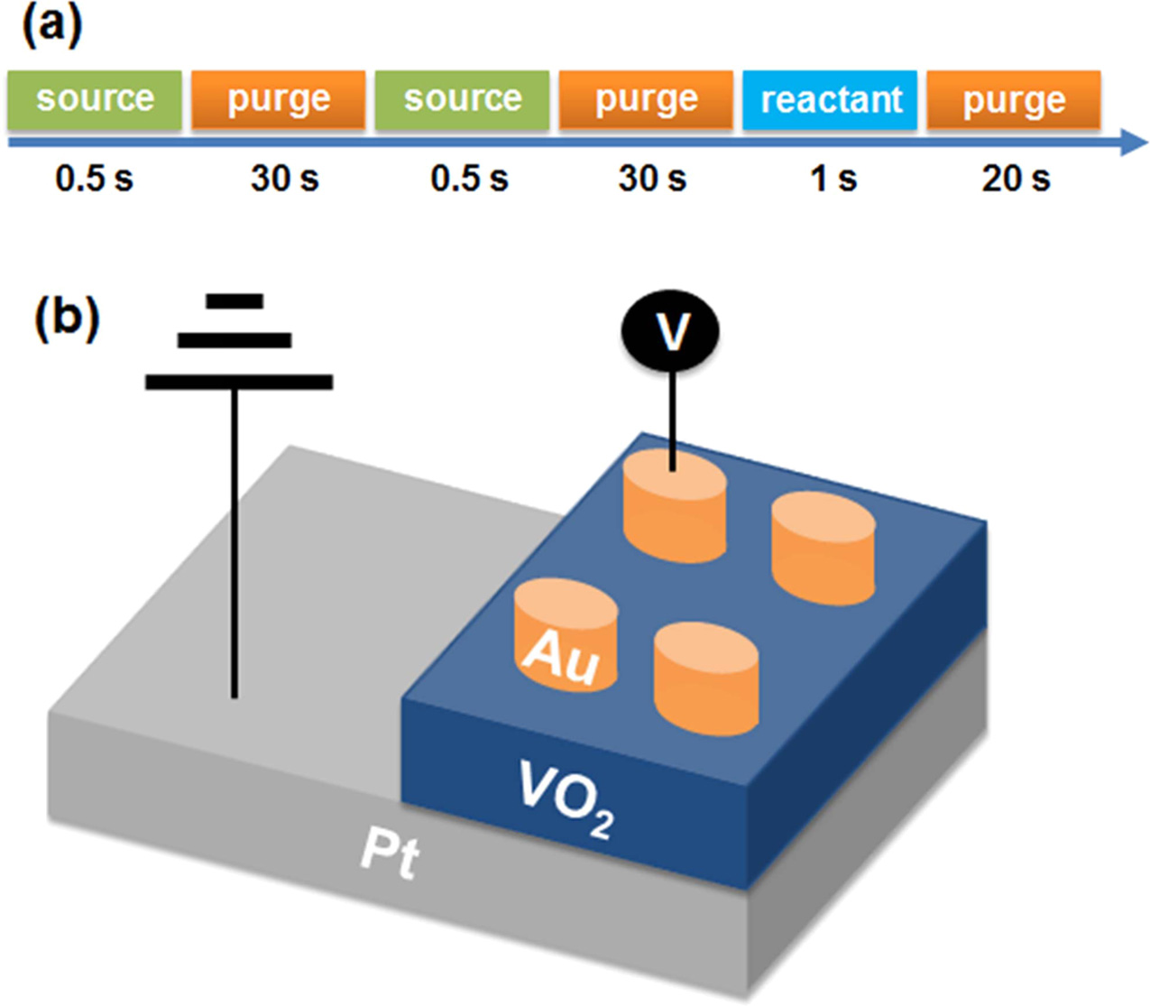
A 20-nm-thick titanium (Ti) adhesion layer was deposited onto a 275 nm SiO2 substrate using an electron beam evaporator. This adhesion layer allows for good platinum (Pt) deposition on the SiO2. After deposition of the adhesion layer, a 70-nm Pt bottom electrode was deposited onto the Ti using electron beam evaporation. Next, monoclinic VO2 thin films with a thickness produced by deposition cycle numbers of 100, 200, and 300 were deposited with thermal ALD employing OV(OCH(CH3)2)3 as the vanadium precursor and water as the reactant. Argon (Ar) gas was injected as the purge gas. The canister of vanadium precursor was kept at 70 oC, and the precursor was injected into the chamber using a bubbler with Ar carrier gas (30 sccm). The deposition temperature was set to 320 oC, and the gas line was kept at 80 oC. The process pressure was maintained at 0.85 Torr (300 sccm purge Ar gas). One cycle of the ALD process consisted of pulse-precursor / purge / pulse-precursor / purge / pulse-water / purge, for respective durations of 0.5 s / 30 s / 0.5 s / 30 s / 1 s / 20 s. A scheme of the ALD process is shown in Fig. 2(a).
For electrical analysis, a metal-insulator-metal (MIM) switching device was fabricated using gold (Au) as the top electrode and Pt as the bottom electrode. After deposition of the VO2 films, a 70-nm-thick Au top electrode was deposited using an electron beam evaporator. The structure of the VO2 MIM device is shown in Fig. 2(b).
After deposition of the VO2 thin film, its crystalline structure was measured by XRD. VO2 thin films were analyzed using 2 theta mode from 10 to 50 o. SEM was conducted to evaluate film thickness and uniformity. To probe chemical bonding of VO2 thin films, XPS analysis was performed to identify the stoichiometry of the vanadium oxide film as either V2O5 or VO2. I-V characteristics of the vanadium oxide films were measured with a semiconductor parameter analyzer at room temperature.
|
Fig. 2 (a) One ALD cycle consisted of pulse-precursor / purge / pulse-precursor / purge / pulse-water / purge (b) Schematic image of a VO2 MIM device. |
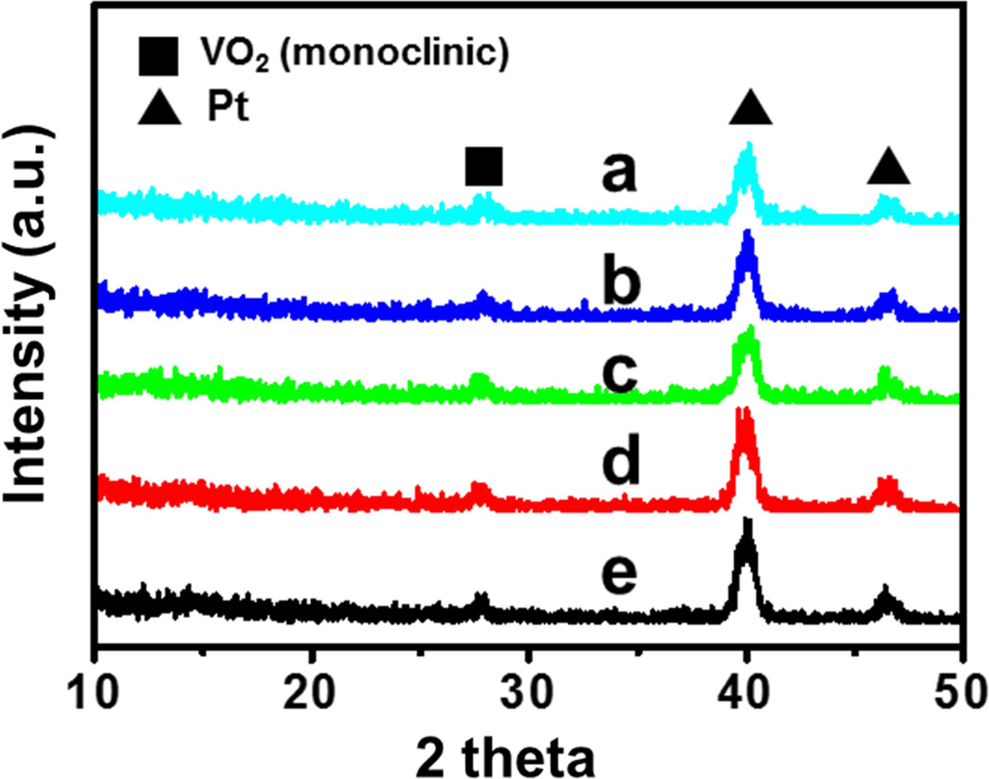
To investigate the presence of VO2 monoclinic phase, we performed an XRD scan from 10 to 50 o using 2 theta mode. Fig. 3 shows XRD profiles through a VO2 / Pt / SiO2 sample to confirm the uniformity of the VO2 thin film. The profiles exhibit three peaks at 28, 40, and 46 o. The VO2 monoclinic peak is observed around 28 o [17], while the Pt peak is observed at 40 and 46 o. The XRD patterns obtained from different locations on the same film show no differences, confirming that thermal ALD with H2O reactant can produce VO2 monoclinic phase films with good crystallinity and uniformity. The grain size of the VO2 thin film calculated using the Scherrer equation and the XRD data was approximately 24.97 nm.
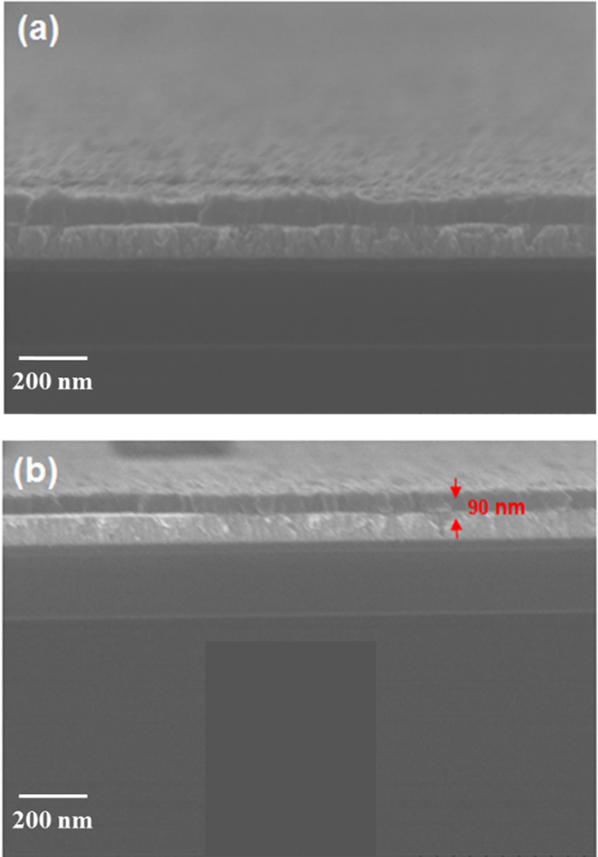
To examine film uniformity, VO2 (300 cycles) / Pt / SiO2 samples with and without split pulse-precursor period were analyzed using SEM. A VO2 sample was deposited without splitting the pulse-precursor period, as seen in Fig. 4(a). Therefore, one ALD cycle used for this sample was pulse-precursor / purge / pulse-water / purge. The process step times correspond to 1 s / 60 s / 1 s / 20 s, respectively. In contrast, a VO2 sample was also deposited by splitting the pulse-precursor period, as shown in Fig. 4(b). In this case, one ALD cycle consists of a pulse-precursor / purge / pulse-precursor / purge / pulse-water / purge with corresponding step times of 0.5 s / 30 s / 0.5 s / 30 s / 1 s / 20 s. Therefore, the total pulse-precursor and purge after pulse-precursor times are the same for both samples. The thin film deposited without a split pulse-precursor period was less uniform and rougher than the film deposited with a split pulse-precursor period. This suggests that the sample deposited without splitting the pulse-precursor period initially grows in island-type mode. Because of this island-type growth mode, there are boundaries between the large VO2 islands, so the thickness of thin film varies over different regions. This result indicates that it is difficult to produce VO2 thin films with uniform thickness when the vanadium precursor is not pulsed separately. In comparison, when VO2 thin film was deposited by splitting the pulse-precursor period, the quality of the thin film improved, as in Fig. 4(b). This sample has excellent uniformity and thin film quality due to film growth under a split pulse-precursor period.
ALD uses self-limiting reactions, a key factor enabling layer by layer thin film growth. At the first step of ALD, a precursor is pulsed and adsorbed onto a substrate, and the ideal first step of surface reaction is that the precursor is perfectly adsorbed onto a substrate. Then, by-products are removed in a subsequent purge step. In practice, however, the precursor does not adsorb perfectly onto the substrate, and by-products are not completely removed in the purge step of ALD. When the precursor is pulsed twice, the pulse time is decreased by about half compared to the unsplit pulse time. Therefore, the amount of precursor exposed to the substrate is half that of the normal pulse cycle, so the number of by-products is small compared to the case of the unsplit pulse precursor. Hence, by-products can be removed completely during the purge step, leaving few impurities on the substrate. Fewer impurities lead to better thin film quality and uniformity compared to thin films deposited using a multi-dosing pulse step in ALD. From the SEM image, the thickness of the VO2 300cycles sample was estimated to be about 90 nm, suggesting that this ALD process had a growth rate of about 0.3 nm / cycle.
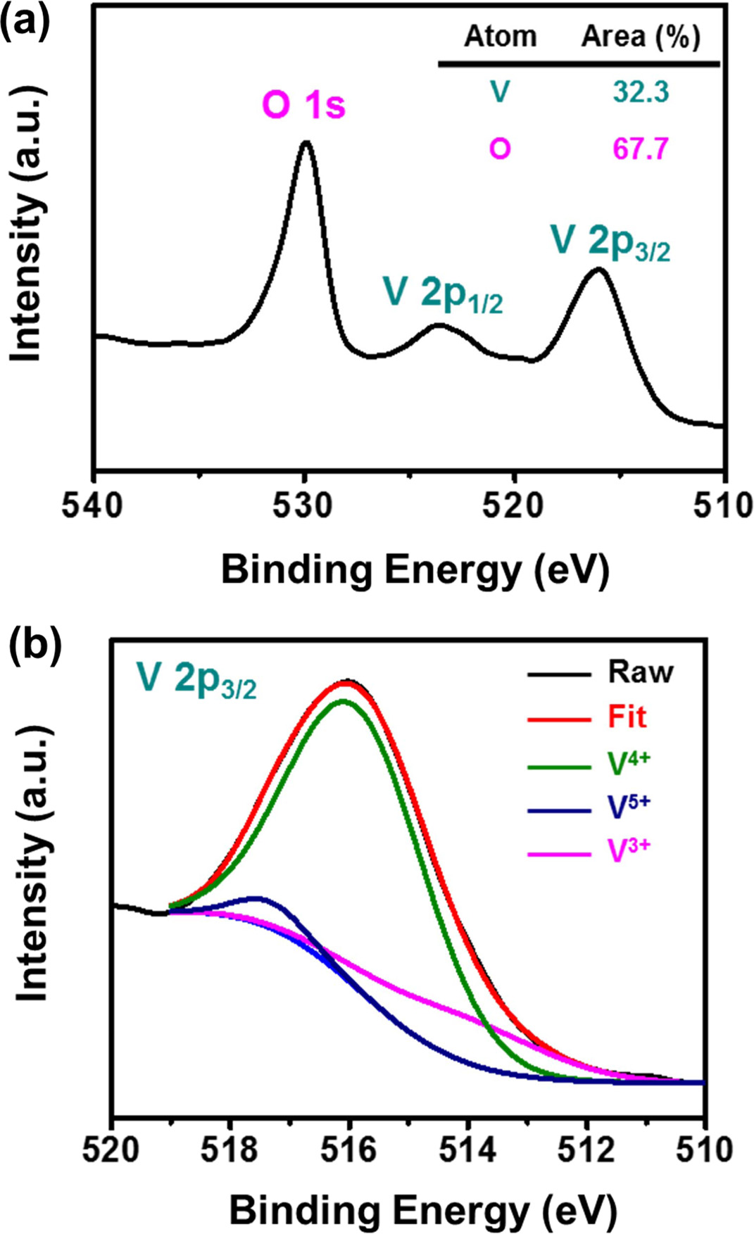
Fig. 5(a) shows the XPS data from a VO2 / Pt / SiO2 sample, which is used to examine the surface chemical states of the deposited films. The binding energies of all XPS spectra were calibrated in reference to the C-C bond in C 1s at 284.6 eV. XPS analysis was performed with and without sample sputtering using Ar ions at 10 mA and 3 kV for about 60 s. After sputtering, no carbon was detected in the samples, indicating that the bulk of VO2 thin films was free of carbon contamination. Fig. 5(b) shows XPS spectra of the de-convoluted V 2p3/2 peak. The V 2p core-level spectra for V2O5, V2O3, and VO2 are different, with oxidation states of 5+, 3+, and 4+, respectively. Generally, binary systems of vanadium and oxygen consist of 25 compounds and suboxide phases. Thus, it has been widely accepted that vanadium oxide compounds are composed of mixed phases such as V2O5, V2O3, and VO2. Accordingly, it is a challenge to obtain a sample of pure VO2 phase. As shown in Fig. 5(b), the V 2p3/2 spectrum is dominated by a 515.99 eV binding energy peak, indicating that the major ionic state of V is V (4+). The O1s peak at 530.0 eV is mostly due to the O-V (4+) binding state [33, 34]. This also confirms that V is fully oxidized to form VO2 when using thermal ALD with H2O reactant. However, stoichiometric analysis using XPS data indicate that the atomic percentages of V and O are 32.3 % and 67.7 %, respectively, indicating that the sample is slightly oxygen-rich VOx (x > 2). It is necessary to reduce the atomic percentage of oxygen with post-treatment.
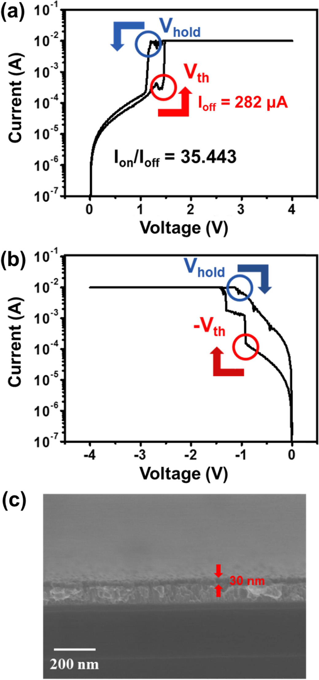
To investigate the electrical characteristics of VO2 as a resistance switching selector, an MIM device, consisting of VO2 thin film produced over 100 ALD cycles and with a top electrode of Au and bottom electrode of Pt, was fabricated. Fig. 6 shows the MIT-based resistance switching property of VO2. When the device is positively biased with increasing voltage from 0 to 4 V (Fig. 6(a)), the current suddenly increases at about 1.4 V, which is called the threshold voltage (Vth). This behavior reveals an electric field-triggered MIT phenomenon as VO2 changes from an insulating state (monoclinic) to a metallic state (tetragonal). On the other hand, positive biasing with decreasing voltage from 4 to 0 V results in a sudden current drop at about 1.2 V. This voltage is the hold voltage (Vhold) and is associated with the electrical properties of VO2 returning to the insulating state. The on (at Vth) / off (at Vhold) current ratio for the selector was about 35. However, the MIT is not observed when the device is biased negatively, as shown in Fig. 6(b), because the VO2 is too thin (i.e., 30 nm as estimated from the SEM image in Fig. 6(c)) to maintain MIT characteristics. Normally, VO2 is deposited using sputter coating or CVD, which create thick VO2 films. Thick VO2 thin films show sustained MIT characteristics, but ALD VO2 thin films are too thin to exhibit such characteristics. The lifetime of a VO2 switching device is proportional to thickness of VO2 thin film. For this reason, MIT characteristics were not observed in the VO2 switching device with a 30-nm-thick VO2 thin film.
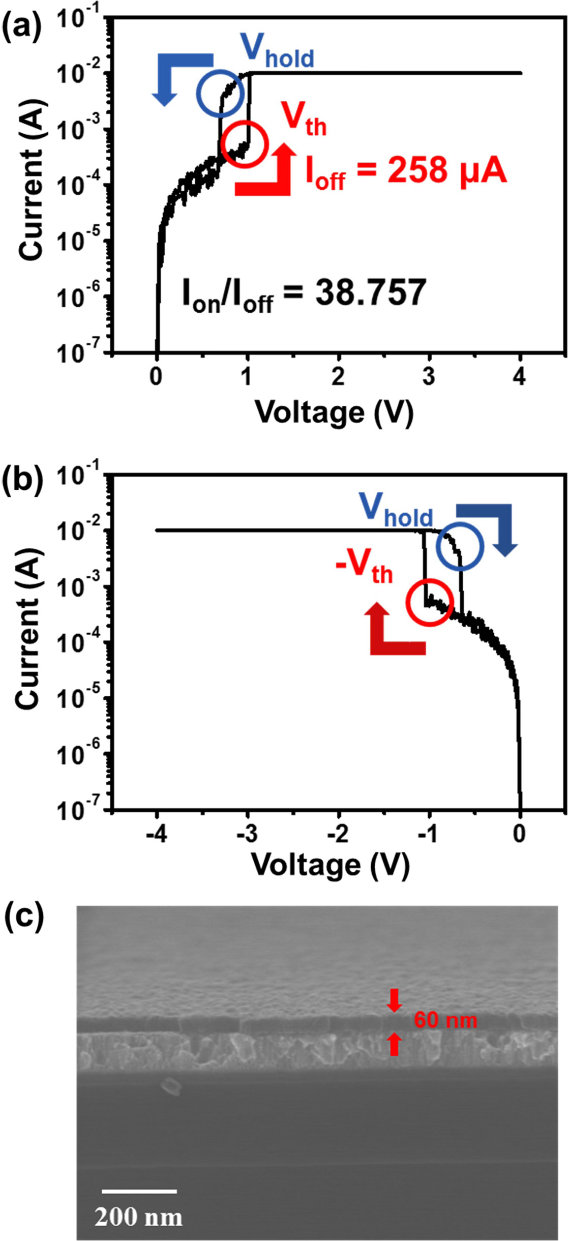
To examine the effect of thickness, a VO2 thin film was deposited over 200 cycles of ALD. The thickness of this film is estimated to be approximately 60 nm from an SEM image (Fig. 7(c)). All other process conditions remained the same in comparison to the film deposited with 100 ALD cycles. Fig. 7 shows the MIT property of this thicker VO2 thin film. Both Vth and Vhold are a bit lower at approximately 0.4 and 0.5 V, respectively, compared to the device with 30-nm-thick VO2. The on/off current ratio slightly increased to about 40. This clearly confirms that the MIM device properties strongly depend on VO2 thickness. In contrast to the 30-nm-thick VO2 device, the MIM device with 60-nm-thick VO2 reveals MIT switching even under negative biasing, with a -Vth of about -1.0 V and a -Vhold of about -0.7 V during a negative bias sweep between 0 and -4 V. It is very interesting that the thicker VO2 sample has lower switching voltages (Vth and Vhold) but a higher on/off current ratio compared to the thinner VO2. This result implies that ability to control the thickness of ALD-grown VO2 films is critical to optimizing the performance of MIT in VO2.
Regarding the long-term cyclic switching performance, the MIM device in this study shows only about 10 cyclic switches, indicating the need for more studies. This result indicates that MIM with 60-nm-thick VO2 has bipolar switching characteristics due to repeatability of MIT switching.
|
Fig. 3 XRD profiles of a VO2 thin film. |
|
Fig. 4 SEM images of VO2 thin film (a) without and (b) with a split pulse-precursor period. |
|
Fig. 5 (a) XPS spectra of the VO2 thin film and (b) the corresponding deconvoluted V 2p3/2 peak. |
|
Fig. 6 I-V characteristics of a VO2 (100 cycles) device at (a) positive, (b) negative voltage, and (c) SEM image of a VO2 (100 cycles) thin film. |
|
Fig. 7 I-V characteristics of a VO2 (200 cycles) device at (a) positive, (b) negative voltage, and (c) SEM image of a VO2 (200 cycles) thin film. |
Atomic layer deposition (ALD) shows various advantages such as excellent step coverage and accurate control of thickness. Here, we report ALD of VO2 thin films for application of MIM-type MIT resistive switching selectors. We demonstrate deposition of a nanoscale VO2 thin film using thermal ALD with H2O reactant. The ALD growth rate of the VO2 thin film is about 0.3 nm / cycle. The developed ALD reveals VO2 phase with good uniformity and film quality based on the material characterization methods XRD, XPS, and SEM. We also present a method for increasing uniformity and thin film quality by splitting the pulse cycle. From electrical analysis of a fabricated MIM device, we demonstrate several noteworthy resistive switching selector parameters, such as Vth and Vhold at about 1 V and on/off current ratio at about 40, driven by the electric field-triggered MIT in the ALD-deposited VO2 thin film. This study suggests the feasibility of fabricating ALD-grown VO2 that shows first-order MIT properties for application in selection devices in cross-point array-type bipolar ReRAMs.
This work was supported by the Nano Material Technology Development Program (2014M3A7B4049367) through the National Research Foundation (NRF) of Korea funded by the Ministry of Science and ICT (MSIT), Korea.
- 1. A. Sawa, Mater. Today 11[6] (2008) 28-36.
-

- 2. R. Waser, R. Dittamann, G. Staikov, and K. Szot, Adv. Mater. 21 (2009) 2632-2663.
-
- 3. H. Jeon, J. Park, W. Jang, H. Kim, C. Kang, H. Song, H. Seo, and H. Jeon, Appl. Phys. Lett. 104 (2014) 151603.
-
- 4. H. Jeon, J. Park, W. Jang, H. Kim, S. Ahn, K.-J. Jeon, H. Seo, and H. Jeon, Carbon 75 (2014) 209-216.
-
- 5. M. Son, J. Lee, J. Park, J. Shin, G. Choi, S. Jung, W. Lee, S. Kim, S. Park, and H. Hwang, IEEE Electron Device Lett. 32[11] (2011) 1579-1581.
-
- 6. M.-J. Lee, Y. Park, D.-S. Suh, E.-H. Lee, S. Seo, D.-C. Kim, R. Jung, B.-S. Kang, S.-E. Ahn, C.B. Lee, D.H. Seo, Y.-K. Cha, I.-K. Yoo, J.-S. Kim, and B.H. Park, Adv. Mater. 19[22] (2007) 3919-3923.
-
- 7. M.-J. Lee, S. Seo, D.-C. Kim, S.-E. Ahn, D.H. Seo, I.-K. Yoo, I.-G. Baek, D.-S. Kim, I.-S. Byun, S.-H. Kim, I.-R. Hwang, J.-S. Kim, S.-H. Jeon, and B.H. Park, Adv. Mater. 19[1] (2007) 73-76.
-
- 8. W.Y. Park, G. H. Kim, J.Y. Seok, K.M. Kim, S.J. Song, M.H. Lee, and C.S. Hwang, Nanotechnology 21 (2010) 195201.
-
- 9. J. Lee, J. Shin, D. Lee, W. Lee, S. Jung, M. Jo, J. Park, K.P. Biju, S. Kim, S. Park, and H. Hwang, Published in 2010 International Electron Devices Meeting, January 2010, DOI: 10.1109/IEDM.2010.5703393.
-
- 10. A. Baikalov, Y.Q. Wang, B. Shen, B. Lorenz, S. Tsui, Y.Y. Sun, Y.Y. Xue, and C.W. Chu, Appl. Phys. Lett. 83 (2003) 957.
-
- 11. Y. Jo, K. Jung, J. Kim, H. Woo, J. Han, H. Kim, J. Hong, J.-K. Lee, and H. Im, Sci. Rep. 4 (2014) 7354.
-
- 12. L. Alekseeva, T. Nabatame, T. Chikyow, and A. Petrov, Jpn. J. Appl. Phys. 55 (2016) 08PB02.
-
- 13. K.-R. Pyon, K.-S. Han, and B.-H. Lee, J. Ceram. Process. Res. 12[3] (2011) 279-288.
- 14. H. Yang, S. Seo. M. Abboudi, and P.H. Holloway, J. Ceram. Process. Res. 8[4] (2007) 256-260
-
- 15. Y. Wang, L. Yang, X. Wang, Y. Wang, and G. Han, J. Ceram. Process. Res. 17[7] (2016) 690-693
- 16. S.-J. Kim, T. Masaki, S.-H. Choi, and D.-H. Yoon, J. Ceram. Process. Res. 17[4] (2016) 338-343
- 17. J. Kim, C. Ko, A. Frenzel, S. Ramanathan, and J.E. Hoffman, Appl. Phys. Lett. 96 (2010) 213106.
-
- 18. S. Zhang, J.Y. Chou, and L.J. Lauhon, Nano Lett. 9[12] (2009) 4257-4532.
-
- 19. J.I. Sohn, H.J. Joo, D. Ahn, H.H. Lee, A.E. Porter, K. Kim, D.J. Kang, and M.E. Welland, Nano Lett. 9[10] (2009) 3392-3397.
-
- 20. J.D. Budai, J. Hong, M.E. Manley, E.D. Specht, C.W. Li, J.Z. Tischler, D.L. Abernathy, A.H. Said, B.M. Leu, L.A. Boatner, R.J. McQueeney, and O. Delaire, Nature 515 (2014) 535-539.
-
- 21. N. Shukal, A.V. Thathachary, A. Agrawal, H. Paik, A. Aziz, D.G. Schlom, S.K. Gupta, R. Engel-Herbert, and S. Datta, Nat. Commun. 6 (2015) 7812.
-
- 22. B. Wang, J. Lai, S. Chen, E. Zhao, H. Hu, and Q. Lu, Opt. Eng. 51[7] (2012) 074003.
-
- 23. F.-W. Yang, K.-H. Chen, C.-M. Cheng, and F.-Y. Su, Ceram. Int. 39 (2013) S729-S732
-
- 24. H. Zhou, J. Li, Y. Xin, G. Sun, S. Bao, and P. Jin, Ceram. Int. 42 (2016) 7655-7663
-
- 25. K. Kosuge, J. Phys. Chem. Solids 28[8] (1967) 1613-1621.
-
- 26. M.B. Sahana, M.S. Dharmaprakash, and S.A. Shivashankar, J. Mater. Chem. 12 (2002) 333–338.
-
- 27. S.J. Yun, J.W. Lim, J.-Su. Noh, B.-G. Chae, and H.-T. Kim, Jpn. J. Appl. Phys. 47 (2008) 3067.
-
- 28. S.-P. Nam, S.-G. Lee, and Y.-H. Lee, J. Ceram. Process. Res. 10[2] (2009) 224-226.
- 29. J. Nag and R.F. Haglund Jr, J. Phys.: Condens. Matter 20 (2008) 264016.
-
- 30. S. Shin, G. Ham, H. Jeon, J. Park, W. Jang, and H. Jeon, Kor. J. Mater. Res. 23 (2013) 405-422.
-
- 31. H.-S. Yun, S.-W. Jung, S.-H. Jeong, K.-H. Kim, C.-A. Choi, and B.-G. Yu, Journal of the Korean Institute of Electrical and Electronic Material Engineers 21 (2008) 156-161.
-
- 32. J. Musschoot, D. Deduytsche, H. Poelman, J. Haemers, R. L. Van Meirhaeghe, S. Van den Berghe, and C. Detavernier, J. Electrochem. Soc. 156[7] (2009) 122-126.
-
- 33. M. Demeter, M. Neumann, and W. Reichelt, Surf. Sci. 454-456 (2000) 41-44.
-
- 34. G. Silversmit, D. Depla, H. Poelman, G.B. Marin, and R.D. Gryse, J. Electron Spectrosc. Relat. Phenom. 135[2-3] (2004) 167-175.
-
 This Article
-
2019; 20(5): 484-489
Published on Oct 31, 2019
- 10.36410/jcpr.2019.20.5.484
- Received on Jun 9, 2019
- Revised on Aug 6, 2019
- Accepted on Aug 14, 2019
Services
- Abstract
introduction
experimental details
results and discussion
conclusion
- Acknowledgements
- References
- Full Text PDF
Shared
Correspondence to
- Hyungtak Seo c , Hyeongtag Jeon a,b
-
aDivision of Nanoscale Semiconductor Engineering, Hanyang University, Seoul, Korea
bDivision of Materials Science and Engineering, Hanyang University, Seoul, Korea
cDepartment of Materials Science and Engineering and Department of Energy Systems Research, Ajou University, Suwon, Korea
Tel : +82-31-219-3532 (H. Seo), +82-22220-0387 (H. Jeon)
Fax: +82-31-219-1613 (H. Seo),+82-2-2292-3523 (H. Jeon) - E-mail: hseo@ajou.ac.kr , hjeon@hanyang.ac.kr
Clean-Energy Research Institute(CRI), Hanyang University, 222, Wangsimni-ro, Seongdong-gu, Seoul, 04763, Korea
E-mail: jcpr@hanyang.ac.kr